| C H A P T E R 5 |
|
Hardware and Functional Description |
This chapter contains the following sections:
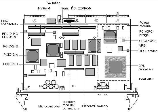
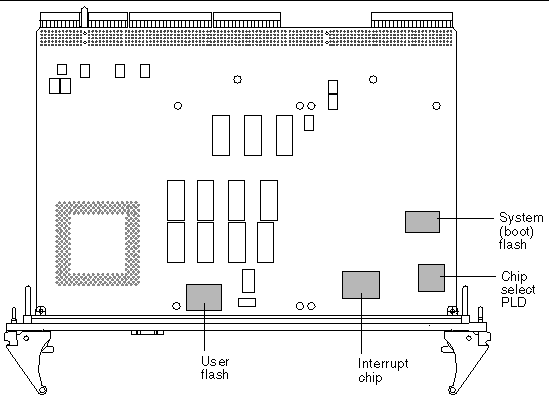
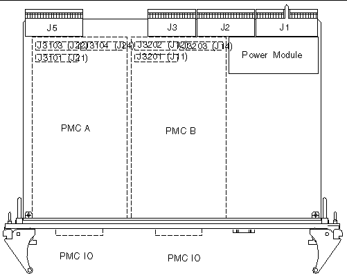
The Netra CP2160 board is a 6U-sized CompactPCI circuit card with CompactPCI connectors J1 and J2 for PCI, and J3 and J5 for I/O. J4 is not fitted to the board. See FIGURE 5-1 and FIGURE 5-2 for top and solder-side views of the board.
FIGURE 5-1 Netra CP2160 Board Layout
|
Note - The heat sink and the power module are shown as dotted lines in this diagram to illustrate the components on the board that lie beneath these devices. |
FIGURE 5-2 Typical Netra CP2160 Board - Solder Side
A Netra CP2160 board functions as a satellite board or as a system host board. The board has the following I/O access:
The front panel of the Netra CP2160 board has two PMC module slots, two Ethernet ports, a serial port and the following reset pushbuttons and status LEDs:
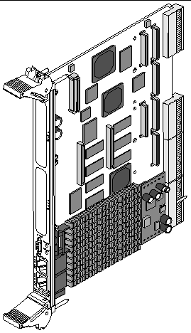
FIGURE 5-3 Typical Netra CP2160 Board Assembly With Heat Sink
A simplified schematic diagram is shown in FIGURE 5-4.
FIGURE 5-4 Netra CP2160 Board Functional Block Diagram
The L2-cache is integrated into the UltraSPARC IIi processor package. This processor is supported by SDRAM memory that is soldered onto the board and is also available in plug-in module form.
Apart from incoming interrupts, the processor handles all I/O through its built-in
66 MHz, 32-bit PCI bus interface. This interface is used to connect to a Sun Advanced PCI Bridge (APB) that services two 33 MHz 32-bit downstream interfaces, PCI bus A and PCI bus B.
PCI bus A connects to a nontransparent PCI bridge (21555 NTB), which services the principal PCI bus connection to the CompactPCI backplane through its connectors J1 and J2. In a system host role, a PCI bus arbiter provides CompactPCI bus arbitration signals for the CPCI backplane bus. It also supplies clocks for the CPCI bus. The arbiter is only active if the system host board is installed into the system slot and functions in a system host role. When the board functions as a satellite board, the CPCI bus arbiter is disabled by the system management controller (SMC). (See Section 5.4.3.1, Arbitration in System Controller Role for details).
PCI Bus B connects the APB to each of two PCIO-2 South Bridge packages, PCIO-2 A and PCIO-2 B. See Section 5.4.2, PCIO-2 Devices and EBus Paths for more details.
In addition, The PCI bus B from the APB connects to each of two 33 MHz, 32-bit PMC interfaces on the host board. See Section 5.4.4, PMC and PIM Interface for more detail.
The SMC controls the startup of the board, because it activates the power module and can control the system reset signals. In addition, it handles hot-swap signals from the CompactPCI backplane, for example: ENUM, HEALTHY, BD_SEL, and PCI_RST (the PCI reset signal). See Section 1.3, Hot-Swap Support for more information on hot-swap.
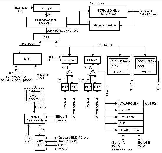
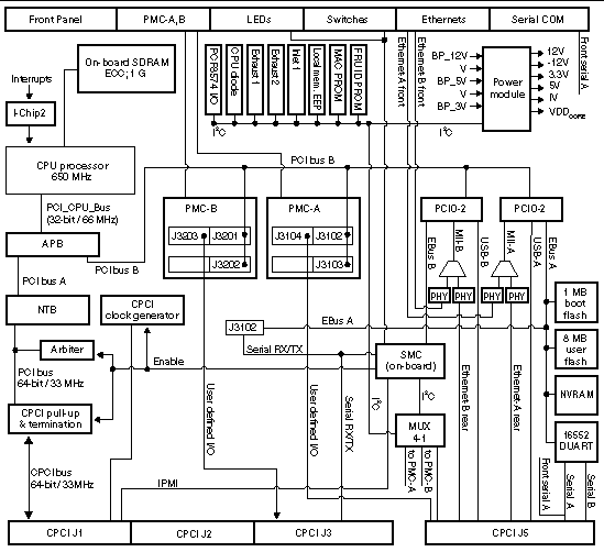
The block schematic diagram of FIGURE 5-5 shows a more detailed block diagram of the Netra CP2160 board.
FIGURE 5-5 Netra CP2160 Board Detailed Block Diagram
This section describes the UltraSPARC-IIi processor and additional memory on the Netra CP2160 boards. FIGURE 5-6 shows the UltraSPARC IIi interfaces.
FIGURE 5-6 UltraSPARC IIi Interface

The Netra CP2160 board uses the UltraSPARC IIi 650 MHz processor. The processor is housed in a 370-pin ceramic pin grid array (PGA) package. It typically dissipates no more than 25 W at 650 Mhz.
The UltraSPARC IIi processor is directly connected to the board SDRAM through a 72-bit ECC path. Dual address buses reduce capacitive loading and increase the memory density beyond that of unbuffered devices.
The CPU connects to the APB by means of a 32-bit, 66 MHz PCI interface which the APB in turn translates to two downstream 33 MHz PCI buses.
The UltraSPARC processor begins execution from a fixed image in a PROM that lies on EBus A. The processor accesses this EBus in a boot path that automatically includes the APB, PCIO-2 A (a South Bridge), and EBus A.
Processor resets are received from the system management controller (SMC). See Section 5.7, Resets and FIGURE 5-20 for more detail.
The various interrupts on the board are prioritized and encoded by the I-chip2 to appear at the UltraSPARC IIi processor as 6-bit parallel data. See Section 5.7, Resets for more information.
The processor I/O is run at a fixed VDDIO of 3.3V but the core voltage, VDDCORE, is adjustable and configured according to CPU speed, typically in the range of 1.3 V to 1.9 V.
JTAG/Test signals are available for use in boundary scan diagnostics.
The UltraSPARC IIi L2 cache megacell reserves a 2 GB region for cacheable main memory. The memory databus width and the module databus width are of equal size (64-bit data plus 8 bit ECC) so memory modules can be installed in mixed sizes.
The UltraSPARC IIi Address Data Generation Logic (ADGL) logically maps modules according to their size, rather than their physical location. The largest sizes are mapped to the lowest address ranges. Where modules of identical size are present, the lower slot number is mapped to the lower address range.
FIGURE 5-7 shows a memory mapping example.
FIGURE 5-7 Memory Mapping Example

FIGURE 5-8 SDRAM Memory Interface
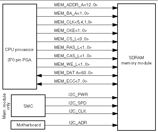
The UltraSPARC IIi 650 MHz processor connects directly to the memory with a 72-bit ECC data bus. The memory can be either on-board SDRAM only or composed of an additional mezzanine memory module.
Each mezzanine memory module has two 100-pin male connectors on its bottom surface--these plug into corresponding female connectors on the system board. No more than one additonal memory modules may be added to the 1 Gbyte on-board memory.
Each module is equipped with a temperature sensor and a serial EEPROM device containing 256 bytes of presence detect data. The double size module (if used) also contains a PLL, which generates eight clock signals. Both the temperature sensor and the serial EEPROM are accessed using the two pin I2C protocol.
The memory block, whether on-board or a module, provides non-volatile serial memory to enable the Serial Presence Detect function. This memory can be interrogated by the SMC through the I2C interface.
This section describes additional memory available on the Netra CP2160 boards.
The system flash resides in 1 Mbyte of space. It contains Common Operations and Reset Environment (CORE) firmware, Comprehensive POST, and OpenBoot PROM boot code. The system flash may be upgraded by running a program out of OpenBoot PROM or executing a Solaris software script. If the system flash becomes corrupted, contact your nearest Field Application Engineer.
The board is equipped with 8 Mbyte of user flash memory. You may use the flash memory for various purposes such as storage for RTOS, user data storage, OpenBoot PROM information, or to house dropins. Dropins simplify customizing a system for the user.
A userflash switch SW2501 determines whether the userflash is detected during OpenBoot PROM boot and whether it is write enabled (see Section B.4, Switch Settings).
The Netra CP2160 board does not have a battery back-up for the NVRAM. The NVRAM on this board functions as SRAM.
These boards use an 8K-bit X 8 timekeeper SRAM (NVRAM) package. This component provides:
This device stores the backup copy of the board MAC address and Host ID in a removable serial EEPROM that is accessible through the I2C bus. This data is downloaded to the SRAM at the OpenBoot PROM level.
The FRU ID I2C EEPROM chip stores manufacturing-related information of the Netra CP2160 board This information is useful only when the Netra board is being serviced.
See Appendix C for details on accessing the FRU ID information for the board.
There are four PCI buses on the board: three internal buses and the external CompactPCI bus that is driven to and from the backplane. One of the internal PCI buses, PCI bus B, is bridged to two lower-speed buses EBus A and EBus B. PCI bus A communicates with the CompactPCI backplane through the nontransparent PCI-to-PCI bridge (21555 NTB). This arrangement is shown in FIGURE 5-9.
FIGURE 5-9 Netra CP2160 Board PCI Bus Interface, 33MHz CompactPCI Bridge
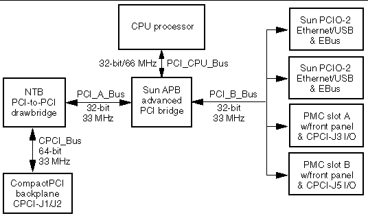
The UltraSPARC IIi CPU has an integrated 32-bit/66 MHz PCI bus interface. The Advanced PCI Bridge--acting as a North Bridge--splits this bus into two
32-bit/33 MHz PCI buses. Of these, the PCI A bus connects to the PCI non-transparent bridge which forms the interface to the CompactPCI backplane. The PCI B bus connects to two PCIO-2 bridges. Each of these bridges carry an EBus and peripheral interfaces at their other end.
The two PCIO-2 bridges connect between the APB PCI Bus B and their EBus and peripheral interfaces at their other end. Each of these bridges carry one EBus interface. The EBus interfaces are used to interface slower internal peripherals.
In addition, PCIO-2 A supports the MII Ethernet A port and USB A port. PCIO-2 B supports the MII Ethernet B port and USB B port.
The nontransparent bridge (NTB), in this case the Intel 21555 device, connects the 32-bit/33 MHz internal PCI bus A to the 64-bit/33 MHz CompactPCI backplane bus through CompactPCI connectors J1 and J2. This interface conforms to the PICMG 2.0 R3.0 CompactPCI Specification. FIGURE 5-10 shows the CompactPCI bus interface.
FIGURE 5-10 CompactPCI Bus Interface
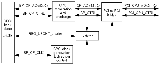
The arbiter--only used when the board functions in a system host board role--provides for orderly sharing of the CompactPCI bus among potential bus masters, or initiators. When the board performs in a system host board role, PCI clocks sourced from a clock generator on the board are driven to a CompactPCI CLK bus signal to all slots on the CompactPCI backplane.
The Netra CP2160 board can be used as a system controller board or as a satellite board. When the Netra board is a system controller board, the arbiter is enabled by the SMC. When the Netra board is a satellite board, the arbiter is disabled by the SMC through a control signal (signal SYS-EN on J2/C2).
FIGURE 5-11 and FIGURE 5-12 illustrate the signal flows for the two board operations.
FIGURE 5-11 Netra CP2160 Board System Controller Board: REQ#/GNT# Signal Flow
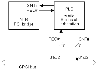
FIGURE 5-12 Netra CP2160 Board Satellite Board: REQ#/GNT# Signal Flow
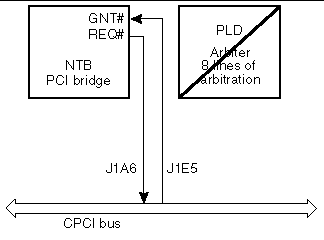
When the Netra CP2160 board is operating as a satellite board, the arbiter is disabled (through a control signal from the SMC module). When disabled, the arbiter tristates REQ1# through REQ6# and GNT1# through GNT6# and pulls them to a known state. The multiplexing, switching, or logic used to control the flow of the arbiter signals comply with all requirements of the CPCI specification, notably the requirements for single loads and stub length.
The PCI mezzanine card (PMC) interface is defined by IEEE and PICMG standards:
The PMC interface enables you to use Independent Hardware Vendor (IHV) PMC to implement additional I/O from the host at the system integration level.
The number of PMCs that can be used with the Netra CP2160 board varies according to the size of modular memory installed on the board. Refer to TABLE 5-1 for details.
A Sun XCP2060-TRN I/O transition card fitted to the rear of the backplane provides slots for PIM cards. A PIM card enables rear I/O functions when paired with a PMC card installed on the front panel of the board.
A PIM must have a corresponding PMC in the front slot because the PMC board performs an adapter function between the PCI bus B and the user I/O signals passed through J5 to the PIM slot on the transition card. When a PMC that has a front-panel connector is used with a PIM, jumpers are typically set to disable its front I/O operation.
FIGURE 5-13 illustrates the interconnection between PMC and PIM slots for installed PIMs.
FIGURE 5-13 PIM Installation Configuration
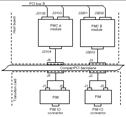
FIGURE 5-14 shows the PMC A and card attachment to a Netra CP2160 board. There is a second PMC connector, PMC B, adjacent to the first (see FIGURE 5-15).
FIGURE 5-14 Data Paths in PCI Mezzanine Module Interface on Host Board
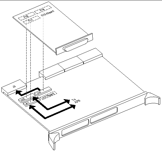
The APB on the Netra CP2160 board supplies PCI bus signals to PMC connectors J21 and J22. The PMC card logic decodes its specific I/O interface, which it makes available at the front panel.
64-pin PMC connectors J23 and J13 are not fitted to these Netra boards. These connectors are specified for expansion for 64-bit PCI (it carries the upper 32 bits), which is not provided. A 64-bit capable PMC card can function in these slots but its bus interface is constrained to 32 bits.
J24 is specified for user I/O and carries PMC signals to CompactPCI backplane connector J3. If a transition card is installed, this J5 I/O is conditioned by an IHV-supplied PIM to provide matching I/O on the enclosure back panel. Its backplane I/O is routed to CompactPCI/J5 connector.
In the case of the PMC B card for the Netra CP2160 board, J11 and J12 are similarly connected to the APB but the user I/O from J14 is routed out of CompactPCI connector J3.
FIGURE 5-15 PMC Connector Interfaces on Netra CP2160 Board.
The I2C paths are shown in FIGURE 5-16. I2C communication is used:
Each I2C device on the board uses common address pins. The devices are distinguished by the internal device ID. All I2C devices are supplied from early power before backend power is established (see Section 5.8, Power Subsystem for further details).
FIGURE 5-16 Netra CP2160 Board and CP2160 I 2 C Paths
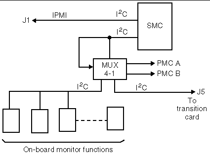
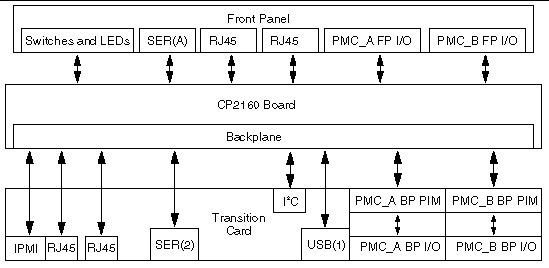
FIGURE 5-17 shows the I/O for the Netra board. The I/O functions can be categorized into four groups which are described in the following sections.
FIGURE 5-18 illustrates the indicators and I/O connectors on the Netra CP2160 board front panel. The Netra CP2160 board front panel connectors, buttons and LEDs are described below:
http://www.sun.com/products-n-solutions/hardware/docs/CPU_Boards/
FIGURE 5-18 Netra CP2160 Board Front Panel
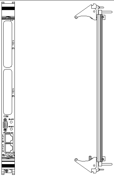
The host board includes two PMC front-panel I/O cutouts to enable attachment of up to two PMC expansion cards. When installed, these cards access a PCI bus through compatible connectors provided on the host board. See Section 5.4.4, PMC and PIM Interface.
Most of the I/O channels to or from the board are passed to CompactPCI connectors J3 and J5; these channels are accessible from external connections on a transition card connected at the rear of the CompactPCI backplane. Connector J4 is not populated on these host boards to prevent contention with H110-compliant backplane signals. Contact assignments for these connectors are shown in Section B.3, CompactPCI Backplane Connectors. For location of the connectors, see FIGURE 5-1.
The user-defined PMC I/O signals from the two PMC Jn3 connectors pass to their external interface through the J3 CompactPCI backplane connector (see Section B.3, CompactPCI Backplane Connectors).
The following signal sets pass through the J5 CompactPCI backplane connector to connect to an external interface connector on the transition card:
The System Management Controller (SMC) subsystem is one of the most important components of the system board. This subsystem provides a variety of service functions related to assuring availability of the system. These functions contrast with the board functions that execute applications.
The SMC consists of a small microcontroller with an SRAM for a software stack and nonvolatile memory for program storage and data logging. The SMC is modular in character, but is physically embedded into the circuitry of the Netra CP2160 board. FIGURE 5-19 shows its functional relationship with the system.
FIGURE 5-19 System Management Controller Interface
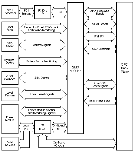
The SMC hardware and firmware implements the functions of system management and hot-swap control.
|
Note - Although the hardware and firmware functions are architecturally separate, reference to the SMC subsystem in this document--whose description is hardware oriented--refers to both functions. |
The SMC controls the on-board CompactPCI interface components for the hot-swap process. It coordinates the state of the 21555 PCI bridge, the arbiter functions, and the switched connection of critical CompactPCI signals to the bus.
In performing these functions, the design maintains conformance with the PICMG CompactPCI core specification and the PICMG CompactPCI hot-swap specification: See Appendix D for references to these documents. The main features that are supported by the SMC subsystem are:
|
Note - This board does not provide HA hot-swap control for peripherals. |
For full details on SMC and reset information, refer to Chapter 4 and the Netra CP2160 board web site:
http://www.sun.com/products-n-solutions/nep/hardware/boards/cp2160/
In the Netra CP2160 board, the SMC implements a two-level watchdog timer. The host-SMC command interface defines communication between host and SMC. The host and the SMC constantly communicate with each other when the watchdog timer is enabled. The SMC monitors the heartbeat of the CPU processor host. The heartbeat is sent in the form of a reset watchdog timer that is sent from the CPU to the SMC. The watchdog timer must be programmed to ensure that it does not get too close to the expiration. There should be some time accounted for the latency overhead or any unexpected event that may delay transmission of the heartbeat. For full details on programming the watchdog timer, refer to the Netra CP2000 and CP2100 Series CompactPCI Boards Programming Guide (816-2485-xx).
The two levels of the watchdog timer are as follows:
The two watchdog timers are enabled by messages sent over the host-SMC command interface using the set watchdog timer command. The commands enabled in the host-SMC command interface for watchdog timer functionality are:
The uses of these functions are shown in TABLE 5-2.
|
Starts and restarts watchdog timer from the initial countdown value |
|
|
Retrieves current settings and present timer value of watchdog timer |
This section provides details on resets for the Netra CP2160 board.
FIGURE 5-20 Simplified Reset Paths
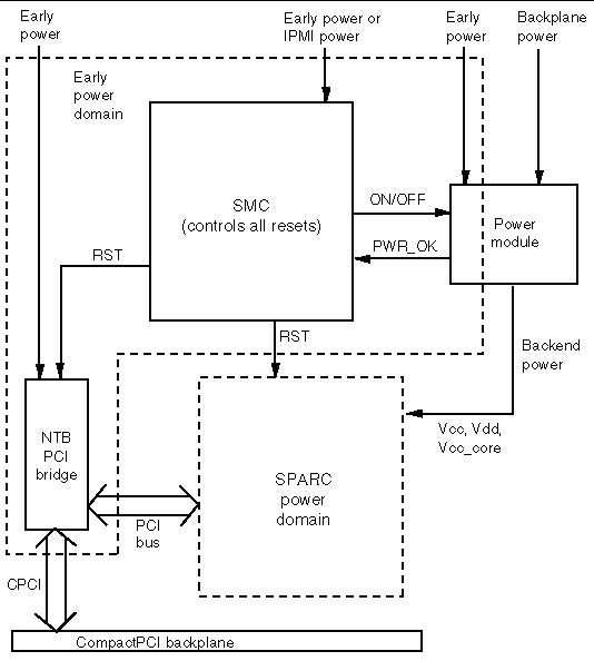
Parts of the system are powered by early power before the SPARC domain receives power (backend power). See Section 5.8, Power Subsystem. At the onset of early power, the SMC is reset by its component microcontroller. When backend power rails are at their specified voltages and if the SMC has the power module turned on, the SMC receives the PWR_OK signal and in turn resets the backend members of the system. Note that:
For detailed information on configurable reset implementation by SMC firmware, see Section 4.7.1, SMC Firmware Reset Modes for System Slot and Peripheral Slot Operations.
FIGURE 5-21 Simplified CPU Subsystem Reset Architecture
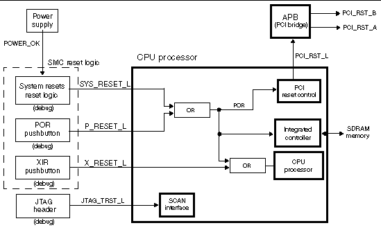
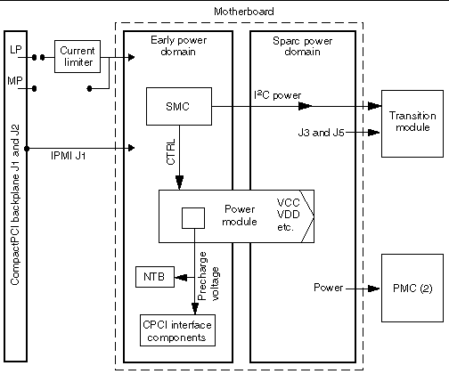
FIGURE 5-22 shows a simplified schematic diagram of the power subsystem. This subsystem can power the board to support a hot-swap environment.
FIGURE 5-22 Power Distribution Block Diagram
|
Note - In FIGURE 5-22 I2C power is derived from early power. |
The Netra CP2160 board sequences power in two time-separated domains:
Early power is applied to the board from backplane long pins (LP in the figure) as the board is inserted. Early power current flows to board subsystems:
FIGURE 5-23 shows a schematic diagram of the power module. This subassembly is integrated with the Netra CP2160 board.
FIGURE 5-23 Power Module Interface
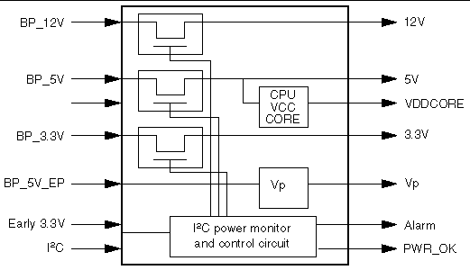
This subsystem performs the following functions:
The power module is controlled by the SMC and the power on/off signal. Functions controlled include core voltage, output level, and module on or off state. There are also automatic controls within the power module, for example, overcurrent shutdown, and voltage regulation.
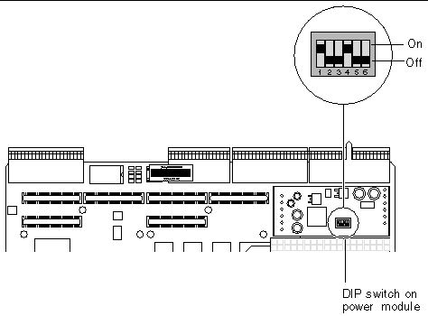
The power module has a DIP switch with six preset default settings. These switches are for factory use only (see FIGURE 5-24 for location). The user must not change DIP switch settings.
FIGURE 5-24 DIP Switch Settings on Power Module
|
Note - The preceding figure is only an example of the types of settings you might find on the board youn receive. The DIP switch settings on your board might have been set differently in the factory. |
If the system power for the backplane fails, the SMC can use IPMI power, typically supplied from an uninterruptible power supply (UPS), instead of early power from the CompactPCI backplane. The backplane is provided with IPMI power pins for this purpose. FIGURE 5-25 shows the circuit arrangement that selects between these power sources.
FIGURE 5-25 Selection Between Early Power and IPMI Power
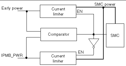
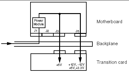
FIGURE 5-26 shows the power rail routing to the transition card. The XCP2160-TRN
I/O transition card is powered from the Netra CP2160 board rather than directly from the backplane. The transition card must always be connected to the backplane before the chassis is powered. Always install the transition card before the Netra CP2160 board in the chassis. For details on using a transition card, see Chapter 3.
FIGURE 5-26 Transition Card Power Supply Routing
|
Note - Some V(I/O) power lines are routed into J2 of the motherboard; this is not shown in the figure for clarity. |
This section provides information on CompactPCI and the Netra CP2160 board interface requirements specifications and CompactPCI signal interface.
TABLE 5-3 lists the requirements for Netra CP2160 boards as defined by the PICMG 3.0 CompactPCI and Netra CP2160 board design requirements specifications:
The tables in this section list the CPCI signal interface description and the CPCI connector power signal interface. The primary side of the bridge is attached to the 64-bit CompactPCI bus.
|
J1-C8, J1-C16, J1-C24, J2-A4, J2-C5, J2-C7, J2-C9, J2-C11, J2-C13 |
|
Note - The early power voltages supply critical circuits such as SMC, CPCI interface circuits, and power module control circuit. |
The Netra CP2160 board interrupts are listed in TABLE 5-6. These are processed and encoded by the I-Chip2 ASIC. This device assigns equal priority to all interrupting devices. When two devices need servicing at the same time, the I-Chip prioritizes using its internal round-robin scheduling scheme. The resultant vector is passed to the processor as a 6-bit parallel word. The ultimate interrupt priority is resolved in the UltraSPARC IIi processor.
|
CPCI_INTA[1] |
|||
|
SPARC_H_INT[2] |
|||
|
SPARC_L_INTSPARC_L_INT and SPARC_H_INT are driven by the SMC module. |
|||
|
CPCI_SERR_L[3] |
|||
The TABLE 5-7 lists the chip-select PLD registers.
|
Note - The registers in the chip-select PLD are mirrored in the EBus address space. |
TABLE 5-8 shows the SMC PLD registers.
Copyright © 2004, Sun Microsystems, Inc. All Rights Reserved.