| Netra CP2140 Technical Reference and Installation Manual |
| Netra CP2140 Technical Reference and Installation Manual |
| C H A P T E R 5 |
|
Functional Description |
This chapter provides a functional description of the Netra CP2140 board, including functional blocks of the board, block diagrams, user interface, and various functions related to Netra CP2140 boards.
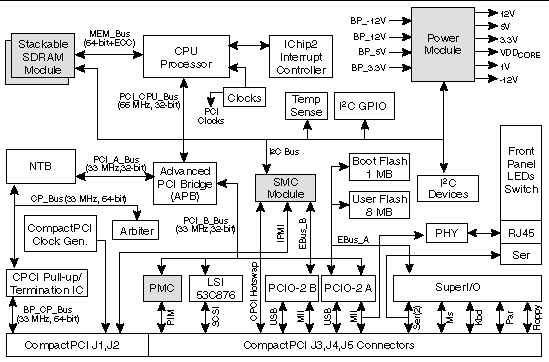
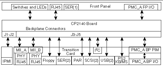
FIGURE 5-1 shows a detailed block diagram of the CP2140.
FIGURE 5-1 Netra CP2140 Board Detailed Block Diagram
|
Note - CP2140 memory and SMC circuits are on mezzanine modules. |
The main functional blocks of the Netra CP2140 board are provided in this section.
FIGURE 5-2 UltraSPARC IIi Interface
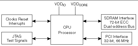
The UltraSPARC IIi 650-MHz processor is based on the 64-bit SPARC V9 architecture. This 4-way superscalar CPU processor has integrated memory controller, PCI controller and 512 KBytes of L2 cache. The processor is directly connected to the board SDRAM through an ECC path.
The Netra CP2140 board has no on-board memory. The memory is composed of up to two mezzanine memory modules. Each mezzanine memory module has two 100-pin male connectors on its bottom surface which plug into corresponding female connectors (J0601 and J0602) on the system board. The module also has two of the same type of female connectors on its top side for memory expansion. Up to two memory modules can be stacked. The CP2140 memory system supports up to two stackable 512 Mbyte/1024 Mbyte Synchronous DRAM (SDRAM) memory modules in any combination.
A 1 Mbyte x 8-bit system flash device resides in one megabyte of space. It contains Common Operations and Reset Environment (CORE) firmware, comprehensive POST, and OpenBoot PROM boot code. The system flash can be upgraded by running a program out of OpenBoot PROM or by executing a Solaris software script. If the system flash becomes corrupted for any reason, contact your Field Application Engineer.
The board is equipped with 8 Mbytes of user flash memory, which is used to house dropins. Dropins simplify customizing a system for the user.
The use an 8 K-bit x 8 timekeeper SRAM (NVRAM) package. This component provides:
|
Note - To ensure proper function, replace NVRAM only with the same or equivalent type recommended by the manufacturer. Dispose off used batteries according to the manufacturer's instructions. |
The serial I2C EEPROM, also called the MAC address carrier, stores the backup copy of the board MAC address and host ID in a removable serial EEPROM that is accessible through the I2C bus. OpenBoot PROM supports retrieving the Ethernet address from the EEPROM, deriving host ID, and downloading this data to the NVRAM. The user can remove and retain this EEPROM for future use in case the board needs to be shipped to the factory for replacement. The replacement board is not shipped with an EEPROM.
TABLE 5-1 shows the clock frequencies on the CP2140 components:.
There are three internal PCI buses on the CP2140:
There is also an external CompactPCI bus driven to and from the backplane.
One of the internal PCI buses, PCI bus B, is bridged to two lower-speed buses: Ebus A and EBus B. PCI bus A communicates with the CompactPCI backplane through the nontransparent PCI bridge (NTB) as shown in FIGURE 5-3.
FIGURE 5-3 Netra CP2140 Board PCI Bus Interface
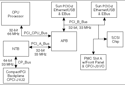
The UltraSPARC IIi processor has an integrated 32-bit, 66 MHz PCI bus interface. The Advanced PCI Bridge (APB) splits this bus into two 32-bit, 33 MHz PCI buses. Of these, the PCI A bus connects to the PCI nontransparent bridge (NTB) which forms the interface to the CompactPCI backplane. The PCI B bus connects to two PCIO-2 bridges. Each of these bridges carries an EBus and peripheral interface at the other end.
The two PCIO-2 bridges connect between two APB devices PCI bus B and their peripheral interfaces at their other ends. Each of these bridges carries one EBus interface. The EBus is similar to the ISA bus and runs at comparable speed. It is used to interface slower internal peripherals.
EBus B connects PCIO-2 B to the System Management Controller (SMC). This path is the primary means of communication between the UltraSPARC IIi host and the SMC and is used to transfer host commands to it.
The UltraSPARC IIi processor expects access to a boot PROM/flash which is normally mapped onto the EBus and requires that the EBus device be directly accessible to the UltraSPARC IIi processor.
FIGURE 5-4 shows the CompactPCI bus interface.
FIGURE 5-4 CompactPCI Bus Interface
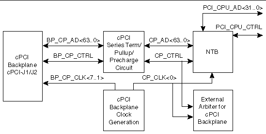
This part of the CP2140 interfaces to the CompactPCI backplane. It is a 64-bit, 33 MHz interface that conforms to the PICMG 2.0 D3.0 Compact PCI Specification and the PICMG 2.1 R1.0 Hot Swap Specification. In order to operate in satellite or nonhost mode, its interface requires the following:
The latter two requirements (series termination and precharge bias) are provided by a custom integrated circuit to save on board space and reduce complexity.
The CompactPCI bus circuit includes a system slot (host CPU) functionality which entails the following:
In addition, the host CPU also provides the Baseboard Management Controller (BMC) functions described in Section 5.3.6, System Management Controller.
As seen in FIGURE 5-1, there are three interfaces to the CompactPCI circuit: the 64-bit CompactPCI backplane, the CompactPCI clock generation, and the output from the bridge onto the PCI_CPU bus.
This section describes the CP2140 system I/O features. FIGURE 5-5 shows the CP2140 I/O interface.
FIGURE 5-5 Netra CP2140 Board I/O Interface
The CP2140 I/O subsystems are onboard SCSI and SuperI/O, which provide two single-ended UltraWide SCSI ports, one parallel port, one floppy port, two serial ports, one keyboard port, and one mouse port.
Each PCIO-2 ASIC provides 10/100BASE-T Ethernet, as well as a USB port.
Access to CP2140 system I/O is provided either partially through the front panel or through the XCP2040-TRN transition card that attaches to the CompactPCI backplane connectors J3-J5 as shown in FIGURE 5-5.
The PMC module provides either front-panel I/O ports or sends user-defined
I/O to the backplane/transition card, where a PIM connector is available to attach the PMC card I/O connector and provide rear-panel I/O access.
I/O to the front panel includes:
I/O through the backplane through the transition card includes:
The PCI Mezzanine Card (PMC) interface is defined by IEEE and PICMG standards. The PMC interface enables independent hardware vendor (IHV) PMC cards to be used to implement a particular I/O interface choice from the host at the system integration level. This choice is independent of any I/O that is provided by the primary hardware. The PMC connectors are provided on the CP2140 to provide modular front panel I/O expansion via a slim mezzanine card mounted parallel to the host computer. This is for user-defined I/O front or back panel access.
|
Note - The Netra CP2140 board supports one PMC card when single-sized memory modules are used. No PMC card is supported with the use of double-sized memory modules. |
A compatible XCP2040-TRN I/O transition card is installed at the rear of the backplane that provides for the attachment of matching IHV-supplied PCI Interface Module (PIM) hardware. The PIM hardware comprises a PMC module which may or may not carry an I/O connector on its front flange. It enables the PIM card to connect to the transition card PIM sockets. These items together can duplicate the PMC front-panel interface at the transition card panel which is at the rear of the enclosure. Examples of such interfaces are a display controller, Ethernet, SCSI, or T1 or T3 communications channels.
FIGURE 5-6 shows the PCI mezzanine module interface on the host board.
FIGURE 5-6 PCI Mezzanine Module Interface on Host Board
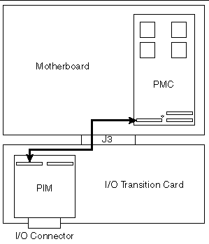
The APB on the CP2140 supplies PCI bus signals to PMC connectors J3001 and J3002. The PMC card logic decodes its specific I/O interface which it makes available at the front panel. J3003 is specified for user I/O and carries PMC signals to CompactPCI backplane connector J3.
FIGURE 5-7 shows the system management controller interface.
FIGURE 5-7 System Management Controller Interface
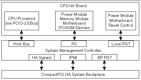
The System Management Controller (SMC) provides two main functions:
As shown in FIGURE 5-7, the SMC interface consists of two parts: the internal/local board interface for ASM and host processor communications, and the interface to the CompactPCI HA/hot-swap backplane.
ASM functions of the SMC include:
Backplane interface functions of the SMC include:
In the Netra CP2140 board, the SMC implements a two-level watchdog timer. The host-SMC command interface defines communication between host and SMC. The host and the SMC constantly communicate with each other when the watchdog timer is enabled. The SMC monitors the heartbeat of the CPU processor host. The heartbeat is sent in the form of reset watchdog timer from the CPU to the SMC. It must be programmed to ensure that it does not get too close to the expiration. There should be some time accounting for the latency overhead or unexpected event that may delay transmission of the heartbeat.
For additional information on the watchdog timer, contact your Field Application Engineer.
The two levels of the watchdog timer are as follows:
The two watchdog timers are enabled by messages sent over the host-SMC command interface using the set watchdog timer command. The commands enabled in the host-SMC command interface for watchdog timer functionality are:
TABLE 5-2 descibes the uses of these functions.
|
Starting-restarting watchdog timer from the initial countdown value |
|
|
Retrieval of current settings and present timer value of watchdog timer |
This section describes the CPU Reset, Reset Modes and Interrupts.
This section lists the reset sequences followed during power on and power off.
The power-on reset process is as follows:
2. POWER_OK is asserted by power supply.
3. System sequences the release of reset.
4. CPU reset is released last.
5. CPU propagates the PCI_RST_L to PCI devices.
6. CPU retrieves the first instruction.
The power-off reset process is as follows:
2. POWER_OK is immediately deasserted.
This section describes the reset modes for system slot and peripheral slot operations for the Netra CP2140 board when used in various roles and CompactPCI slots.
TABLE 5-3 describes the available modes of operation in response to a reset request on the CompactPCI backplane. Determination of system or peripheral slot/satellite operation is made from the state of the CompactPCI backplane SYSEN# signal as specified in the PICMG 2.0 R 3.0 Specification. Note that the RESET# signal has no effect on the System Management Bus or its associated Intelligent Peripheral Microcontrollers.
The default setting for the Netra CP2140 board is mode 66, giving standard system controller operation when the board is installed in the system slot and standalone operation for use in peripheral/satellite slots.
FIGURE 5-8 shows the simplified Reset paths.
FIGURE 5-8 Simplified Reset Paths
Portions of the system are powered by early power before the SPARC domain receives power (backend power). See Section 5.5, Power Subsystem. At the onset of early power, the SMC is reset.
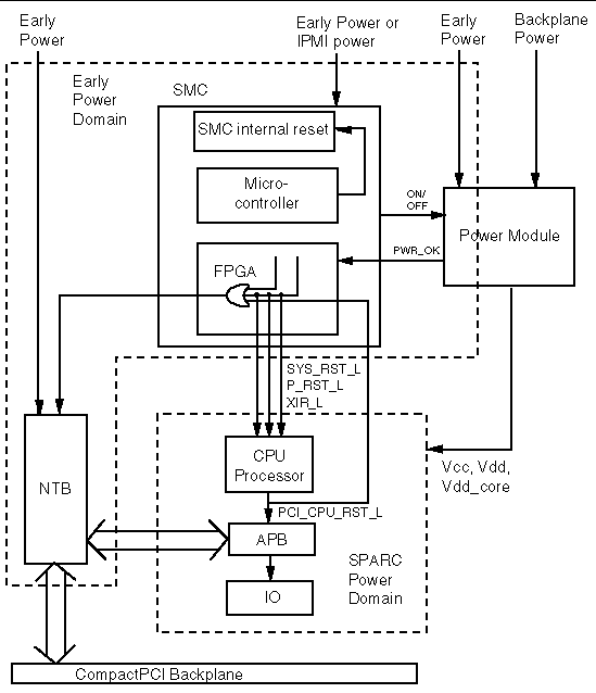
FIGURE 5-9 shows a simplified diagram of the power subsystem. This subsystem provides for powering the Netra CP2140 board in a way that supports a hot-swap environment.
FIGURE 5-9 Power Distribution Block Diagram
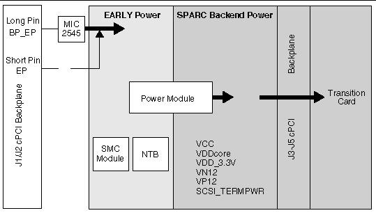
The CP2140 sequences power in two time-separated domains:
Early power is applied to the board from backplane long pins as the board is inserted. Early power current flows to board subsystems:
The power module subassembly is a self-contained DC/DC converter with an on-board hot-swap controller for the CompactPCI voltages +/-12V, 5V, and 3.3V. The power module is controlled by the SMC using the local I2C bus. Monitoring tasks also are implemented over the I2C bus. Functions controlled by SMC include core voltage, output level, and module on or off state. Within the power module, there are automatic controls such as overcurrent shutdown and voltage regulation.
This subsystem performs the following functions:
This module uses early power from the backplane to provide precharge voltage for the NTB and other CompactPCI interface hardware. The remaining power rails are activated by the SMC after the board is fully inserted into the backplane. When these rails have stablized, the PWR_MOD_OK signal does the following:
In the event of a failure of system power for the backplane, the SMC can use IPMI Power, typically supplied from an uninterruptible power supply (UPS), instead of Early Power from the CompactPCI backplane.
FIGURE 5-10 shows the circuit arrangement that selects between these power sources.
FIGURE 5-10 Selection Between Early Power and IPMI Power
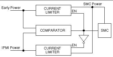
The comparator monitors Early Power and IPMI Power and enables one of the current limiters--based upon MOSFET switches--at a time. When Early Power voltage drops below specification, its supply to the board is disabled and the IPMI Power MOSFET switch is turned on, passing that supply to the load instead. Restoration of Early Power returns the switches to their original states.
This section provides hot-swap architecture information and a description of the different hot-swap models.
In general, hot swapping is the capability or property of a system element to be removed or replaced while the system hardware is nominally operating under power. The objectives in introducing hot-swap capability to a CompactPCI system include the following:
There are three levels of hot swap:
Basic: Provides hardware features required to perform hot swap, but operator intervention is required to execute software steps such as system configuration and installation of device drivers.
Full Hot Swap: Provides both hardware and software features required for software connection control. Board software connection control resources provide the following:
High Availability (HA): In an HA system, hardware and software is added to enable a higher degree of system control. The following signals are issued to control each slot in the system:
The arbiter in the PLD provides arbitration of the CompactPCI bus interface with SMC optional boot flash PROM interfaces. As a system controller, the arbiter receives seven requests from the CompactPCI bus and one request from the NTB. The arbiter processes the eight requests based on a round-robin arbitration scheme. As a satellite, the arbiter is disabled and the system passes the NTB request to CompactPCI request 0 and passes CompactPCI grant 0 to 21555 request.
| Netra CP2140 Technical Reference and Installation Manual | 816-4908-10 |
Copyright © 2002, Sun Microsystems, Inc. All rights reserved.