| Netra CT 820 Server Installation Guide
|
   
|
This chapter gives instructions for connecting cables to the cards. It is divided into the following sections:
Connecting Cables to the Distributed Management Cards
The Netra CT 820 server is available only as a rear-access server, so most of the cabling for the distributed management card will be to the rear transition card at the rear of the server. The only exception would be the console port on the distributed management card at the front of the server. You can administer the Netra CT 820 server either from the front of the server, through the console port on the distributed management card, or from the rear of the server, through one of the two console ports on the rear transition card.

|
Caution - Do not attempt to administer the Netra CT 820 server through the console ports on both the distributed management card and the rear transition card at the same time. No mechanism is provided to disable simultaneous input from the front and rear cards, so attempts to input data from both ports will place the boards in an unknown state.
|
Ports on the Distributed Management Card
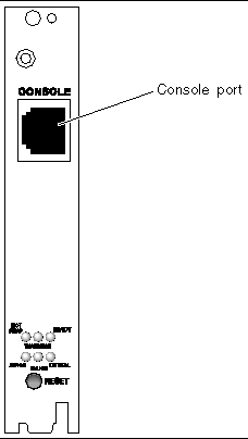
FIGURE 4-1 shows the location of the console port on the distributed management card. The pinouts for the console port on the distributed management card are given in Console Port.
FIGURE 4-1 Location of the Console Port on the Distributed Management Card
Console Port
The console port on the distributed management card uses a standard RJ-45 connector.
FIGURE 4-2 RJ-45 Console Port Diagram

TABLE 4-1 Console Port Pinouts
|
Pin No.
|
Description
|
Pin No.
|
Description
|
|
1
|
RTS
|
5
|
DCD
|
|
2
|
DTR
|
6
|
RXD
|
|
3
|
TXD
|
7
|
DSR
|
|
4
|
GND
|
8
|
CTS
|
Ports on the Rear Transition Card for the Distributed Management Card
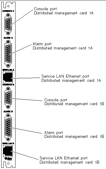
FIGURE 4-3 shows the ports on the rear transition card for the distributed management cards. Note that a single rear transition card gives ports for both of the distributed management cards installed in the front of the server (1A and 1B).
FIGURE 4-3 Distributed Management Card Rear Transition Module Ports
 [ D ]
[ D ]
Following are the pinouts for each of the ports on the rear transition module for the distributed management card:
Console Ports 1A and 1B
The console ports 1A and 1B on the rear transition card for the distributed management card use standard DB-9 connectors.
FIGURE 4-4 Console Port Connector Pins

The signal interfaces of the connectors are described in the following two tables.
TABLE 4-2 Console Port 1A
|
Pin No.
|
Signal
|
Pin No.
|
Signal
|
|
1
|
COM_A_DCD
|
6
|
COM_A_DSR
|
|
2
|
COM_A_RXD
|
7
|
COM_A_RTS
|
|
3
|
COM_A_TXD
|
8
|
COM_A_CTS
|
|
4
|
COM_A_DTR
|
9
|
COM_A_RI
|
|
5
|
GND_A
|
|
|
TABLE 4-3 Console Port 1B
|
Pin No.
|
Signal
|
Pin No.
|
Signal
|
|
1
|
COM_B_DCD
|
6
|
COM_B_DSR
|
|
2
|
COM_B_RXD
|
7
|
COM_B_RTS
|
|
3
|
COM_B_TXD
|
8
|
COM_B_CTS
|
|
4
|
COM_B_DTR
|
9
|
COM_B_RI
|
|
5
|
GND_B
|
|
|
Alarm Ports 1A and 1B
The alarm ports 1A and 1B on the rear transition module for the distributed management card use standard male DB-15 connectors.
FIGURE 4-5 Alarm Port

TABLE 4-4 Alarm Ports 1A and 1B Pinouts
|
Pin No.
|
Signal
|
Pin No.
|
Signal
|
Pin No.
|
Signal
|
|
1
|
RESET0 +
|
6
|
ALARM0_NC
|
11
|
ALARM2_NO
|
|
2
|
RESET0 -
|
7
|
ALARM0_COM
|
12
|
ALARM2_NC
|
|
3
|
RESET1 +
|
8
|
ALARM1_NO
|
13
|
ALARM2_COM
|
|
4
|
RESET1 -
|
9
|
ALARM1_NC
|
14
|
ALARM3_NO
|
|
5
|
ALARM0_NO
|
10
|
ALARM1_COM
|
15
|
ALARM3_COM
|
Ethernet Ports 1A and 1B
The Ethernet ports 1A and 1B on the rear transition module for the distributed management card use standard RJ-45 connectors. They are both 10 Mbit/sec Ethernet ports.
|
Note - The external Ethernet interface on the distributed management card and the external Ethernet interface on the switching fabric board must be connected to different subnets. If they are configured on the same subnet, arp messages will be displayed on the distributed management card console.
|
FIGURE 4-6 RJ-45 Ethernet Connector Diagram

TABLE 4-5 Ethernet Ports 1A and 1B Pinouts
|
Pin No.
|
Description
|
Pin No.
|
Description
|
|
1
|
TX+
|
5
|
Not used
|
|
2
|
TX-
|
6
|
RX-
|
|
3
|
RX+
|
7
|
Not used
|
|
4
|
Not used
|
8
|
Not used
|
Connecting Cables to the Switching Fabric Boards
|
Note - If you want the Ethernet signals to be routed to the rear transition card for the switching fabric board, verify that the SW503 DIP switch on the Netra CP2300 board is set correctly. See Ethernet Networking on the Netra CP2300 Board for more information before proceeding with these instructions.
|
|
Note - The external Ethernet interface on the distributed management card and the external Ethernet interface on the switching fabric board must be connected to different subnets. If they are configured on the same subnet, arp messages will be displayed on the distributed management card console.
|
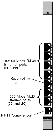
The Netra CT 820 server is available only as a rear-access server, so all of the cabling for the switching fabric board will be to the rear transition card at the rear of the server. There are no active components on the rear transition card, so you must have the accompanying switching fabric board installed in the same slot at the front of the server, even though no cables will be connected to that front card. The rear transition card is connected to the switching fabric board through the midplane through the RJ3 and RJ5 CompactPCI connectors. This card used to route Ethernet traffic through five 10/100-megabit switched Ethernet MDIX ports through shielded RJ-45 connectors (ports 20-23), two 1000-megabit Ethernet MDIX ports (ports 25-26), and an RJ-11 console port. FIGURE 4-7 shows the ports on the rear transition card for the switching fabric board.
|
Note - Port 24 on the rear transition card for the switching fabric board is reserved for future use.
|
FIGURE 4-7 Ports on the Rear Transition Card for the Switching Fabric Board
 [ D ]
[ D ]
Following are the pinouts for each of the ports on rear transition card for the switching fabric board:
10/100 Mbit/sec Ethernet Ports (20-23)
The Ethernet ports 20-23 on the rear transition module for the switching fabric board use standard RJ-45 connectors. They are all 10/100 Mbit/sec Ethernet ports.
FIGURE 4-8 RJ-45 Ethernet Connector Diagram

TABLE 4-6 10/100Mb Switched Ethernet Port Pinout
|
Pin No.
|
Signal
|
Pin No.
|
Signal
|
|
1
|
RX+
|
5
|
--
|
|
2
|
RX-
|
6
|
TX-
|
|
3
|
TX+
|
7
|
--
|
|
4
|
--
|
8
|
--
|
1000 Mbit/sec Ethernet Ports (25 and 26)
The Ethernet ports 25 and 26 on the rear transition module for the switching fabric board use standard RJ-45 connectors. They are both 1000 Mbit/sec Ethernet ports.
FIGURE 4-9 RJ-45 Ethernet Connector Diagram
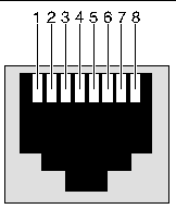
TABLE 4-7 1000Mb Switched Ethernet Port Pinout
|
Pin No.
|
Signal
|
Pin No.
|
Signal
|
|
1
|
TRDB+
|
5
|
TRDD-
|
|
2
|
TRDB-
|
6
|
TRDA-
|
|
3
|
TRDA+
|
7
|
TRDC+
|
|
4
|
TRDD+
|
8
|
TRDC-
|
Console Port
The console port on the rear transition module for the switching fabric board uses a standard RJ-11 connector. A special cable for connection with the console port is included in the Netra CT 820 server ship kit.
FIGURE 4-10 RJ-11 Console Connector Diagram
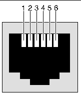
The only signals used are transmit, receive, and ground. The pinouts for this port is shown in TABLE 4-8.
TABLE 4-8 RJ11 Console Port Pinout
|
RJ11
Pin Number
|
Signal Name
|
DCE DB-9
Pin Number
|
DTE DB-9
Pin Number
|
|
1
|
--
|
--
|
--
|
|
2
|
GND
|
5
|
5
|
|
3
|
RX
|
3
|
2
|
|
4
|
TX
|
2
|
3
|
|
5
|
GND
|
--
|
--
|
|
6
|
--
|
--
|
--
|
|
Note - DTE DB-9 also provides loopback of DTR (pin 4) to DSR (pin 6) and of RTS (pin 8) to CTS (pin 9).
|
Connecting the Cables to the Netra CP2300 Boards
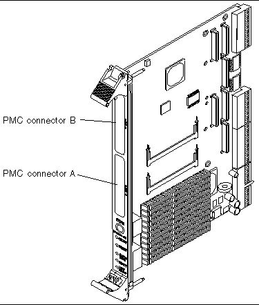
The Netra CT 820 server is available only as a rear-access server, so all of the cabling for the Netra CP2300 boards will be to the rear transition card at the rear of the server. However, in order to use the PCI Interface Modules (PIMs) on the rear transition card, you must also have the accompanying PCI mezzanine cards (PMCs) installed on the Netra CP2300 board.
PMCs on the Netra CP2300 Board
FIGURE 4-11 shows the location of the PMCs on the Netra CP2300 board, and PMC Connectors gives connector interface information for the PMC slots.
\
FIGURE 4-11 Netra CP2300 Board
PMC Connectors
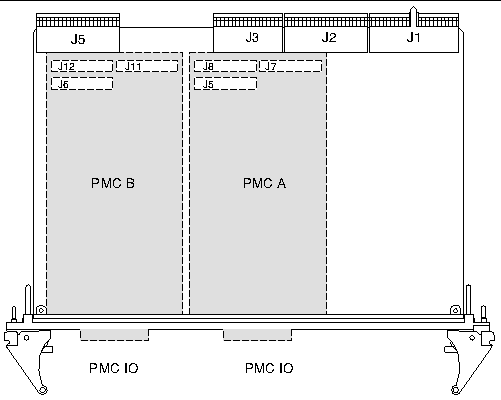
FIGURE 4-12 shows the locations of PMC port connectors. The following tables show contact allocations.
FIGURE 4-12 Netra CP2300 Board PMC Port Connectors
|
Note - The P1386.1 standard reserves the Jn3 64-pin connector for PCI 64-bit extensions, so it is not fitted on the Netra CP2300 board.
|
PMC B Connector Interfaces
The PMC B connector interface consists of three connectors: J6, J12, and J11. These connectors conform to the common mezzanine card (CMC) specification.
TABLE 4-9 PMC B J6 Connector Interface
|
Pin
|
Description
|
Pin
|
Description
|
|
1
|
TCK; JTAG clock signal.
|
2
|
-12V
|
|
3
|
GND
|
4
|
PMC_B_INT_A_L
|
|
5
|
PMC_B_INT_B_L
|
6
|
PMC_B_INT_C_L
|
|
7
|
PMC_BUSMODE1_L
|
8
|
VCC (5V)
|
|
9
|
PMC_B_INT_D_L
|
10
|
NC
|
|
11
|
GND
|
12
|
NC
|
|
13
|
PMC_CLK
|
14
|
GND
|
|
15
|
GND
|
16
|
PMC_GNT_L
|
|
17
|
PMC_REQ_L
|
18
|
VCC
|
|
19
|
LOCAL_VIO
|
20
|
PCI_B_AD<31>
|
|
21
|
PCI_B_AD<28>
|
22
|
PCI_B_AD<27>
|
|
23
|
PCI_B_AD<25>
|
24
|
GND
|
|
25
|
GND
|
26
|
PCI_B_CBE3_L
|
|
27
|
PCI_B_AD<22>
|
28
|
PCI_B_AD<21>
|
|
29
|
PCI_B_AD<19>
|
30
|
VCC
|
|
31
|
LOCAL_VIO
|
32
|
PCI_B_AD<17>
|
|
33
|
PCI_B_FRAME_L
|
34
|
GND
|
|
35
|
GND
|
36
|
PCI_B_IRDY_L
|
|
37
|
PCI_B_DEVSEL_L
|
38
|
VCC
|
|
39
|
GND
|
40
|
PCI_B_LOCK_L
|
|
41
|
PMC_SDONE
|
42
|
PMC_SB0_L
|
|
43
|
PCI_B_PAR
|
44
|
GND
|
|
45
|
LOCAL_VIO
|
46
|
PCI_B_AD<15>
|
|
47
|
PCI_B_AD<12>
|
48
|
PCI_B_AD<11>
|
|
49
|
PCI_B_AD<9>
|
50
|
VCC
|
|
51
|
GND
|
52
|
PCI_B_CBE_L<0>
|
|
53
|
PCI_B_AD<6>
|
54
|
PCI_B_AD<5>
|
|
55
|
PCI_B_AD<4>
|
56
|
GND
|
|
57
|
LOCAL_VIO
|
58
|
PCI_B_AD<3>
|
|
59
|
PCI_B_AD<2>
|
60
|
PCI_B_AD<1>
|
|
61
|
PCI_B_AD<0>
|
62
|
VCC
|
|
63
|
GND
|
64
|
PCI_B_REQ64_L
|
TABLE 4-10 PMC B J12 Connector Interface
|
Description
|
Pin
|
Pin
|
Description
|
|
+12V
|
1
|
2
|
JTAG_PMC_RST_L
|
|
TMS
|
3
|
4
|
PMC_TDO
|
|
PMC_TDI
|
5
|
6
|
GND
|
|
GND
|
7
|
8
|
NC
|
|
NC
|
9
|
10
|
NC
|
|
PMC_BUSMODE2_L
|
11
|
12
|
VDD (3.3V)
|
|
PCI_B_RST_L
|
13
|
14
|
PMC_BUSMODE3_L
|
|
VDD
|
15
|
16
|
PMC_BUSMODE4_L
|
|
NC
|
17
|
18
|
GND
|
|
PCI_B_AD<30>
|
19
|
20
|
PCI_B_AD<29>
|
|
GND
|
21
|
22
|
PCI_B_AD<26>
|
|
PCI_B_AD<24>
|
23
|
24
|
VDD
|
|
PCI_B_IDSEL
|
25
|
26
|
PCI_B_AD<23>
|
|
VDD
|
27
|
28
|
PCI_B_AD<20>
|
|
PCI_B_AD<18>
|
29
|
30
|
GND
|
|
PCI_B_AD<16>
|
31
|
32
|
PCI_B_CBE_L<2>
|
|
GND
|
33
|
34
|
NC
|
|
PCI_B_TRDY_L
|
35
|
36
|
VDD
|
|
GND
|
37
|
38
|
PCI_B_STOP_L
|
|
PCI_B_PERR_L
|
39
|
40
|
GND
|
|
VDD
|
41
|
42
|
PCI_B_SERR_L
|
|
PCI_B_CBE_L<1>
|
43
|
44
|
GND
|
|
PCI_B_AD<14>
|
45
|
46
|
PCI_B_AD<13>
|
|
GND
|
47
|
48
|
PCI_B_AD<10>
|
|
PCI_B_AD<8>
|
49
|
50
|
VDD
|
|
PCI_B_AD<7>
|
51
|
52
|
NC
|
|
VDD
|
53
|
54
|
NC
|
|
NC
|
55
|
56
|
GND
|
|
NC
|
57
|
58
|
NC
|
|
GND
|
59
|
60
|
NC
|
|
PCI_B_ACK64_L
|
61
|
62
|
VDD
|
|
GND
|
63
|
64
|
NC
|
TABLE 4-11 PMC B J11 Connector Interface
|
Pin
|
Description
|
|
1-64
|
PMC_B_IO<1-64> are user-defined IO pins
|
PMC A Connector Interfaces
The PMC A connector interface consists of three connectors: J5, J8, and J7. These connectors conform to the common mezzanine card (CMC) specification.
TABLE 4-12 PMC A J5 Connector Interface
|
Pin
|
Description
|
Pin
|
Description
|
|
1
|
TCK; JTAG clock signal.
|
2
|
-12V
|
|
3
|
GND
|
4
|
PMC_A_INT_A_L
|
|
5
|
PMC_A_INT_B_L
|
6
|
PMC_A_INT_C_L
|
|
7
|
PMC_BUSMODE1_L
|
8
|
VCC (5V)
|
|
9
|
PMC_A_INT_D_L
|
10
|
NC
|
|
11
|
GND
|
12
|
NC
|
|
13
|
PMC_CLK
|
14
|
GND
|
|
15
|
GND
|
16
|
PMC_GNT_L
|
|
17
|
PMC_REQ_L
|
18
|
VCC
|
|
19
|
LOCAL_VIO
|
20
|
PCI_B_AD<31>
|
|
21
|
PCI_B_AD<28>
|
22
|
PCI_B_AD<27>
|
|
23
|
PCI_B_AD<25>
|
24
|
GND
|
|
25
|
GND
|
26
|
PCI_B_CBE3_L
|
|
27
|
PCI_B_AD<22>
|
28
|
PCI_B_AD<21>
|
|
29
|
PCI_B_AD<19>
|
30
|
VCC
|
|
31
|
LOCAL_VIO
|
32
|
PCI_B_AD<17>
|
|
33
|
PCI_B_FRAME_L
|
34
|
GND
|
|
35
|
GND
|
36
|
PCI_B_IRDY_L
|
|
37
|
PCI_B_DEVSEL_L
|
38
|
VCC
|
|
39
|
GND
|
40
|
PCI_B_LOCK_L
|
|
41
|
PMC_SDONE
|
42
|
PMC_SB0_L
|
|
43
|
PCI_B_PAR
|
44
|
GND
|
|
45
|
LOCAL_VIO
|
46
|
PCI_B_AD<15>
|
|
47
|
PCI_B_AD<12>
|
48
|
PCI_B_AD<11>
|
|
49
|
PCI_B_AD<9>
|
50
|
VCC
|
|
51
|
GND
|
52
|
PCI_B_CBE_L<0>
|
|
53
|
PCI_B_AD<6>
|
54
|
PCI_B_AD<5>
|
|
55
|
PCI_B_AD<4>
|
56
|
GND
|
|
57
|
LOCAL_VIO
|
58
|
PCI_B_AD<3>
|
|
59
|
PCI_B_AD<2>
|
60
|
PCI_B_AD<1>
|
|
61
|
PCI_B_AD<0>
|
62
|
VCC
|
|
63
|
GND
|
64
|
PCI_B_REQ64_L
|
TABLE 4-13 PMC A J8 Connector Interface
|
Pin
|
Description
|
Pin
|
Description
|
|
1
|
+12V
|
2
|
JTAG_PMC_RST_L
|
|
3
|
TMS
|
4
|
PMC_TDO
|
|
5
|
PMC_TDI
|
6
|
GND
|
|
7
|
GND
|
8
|
NC
|
|
9
|
NC
|
10
|
NC
|
|
11
|
PMC_BUSMODE2_L
|
12
|
VDD (3.3V)
|
|
13
|
PCI_B_RST_L
|
14
|
PMC_BUSMODE3_L
|
|
15
|
VDD
|
16
|
PMC_BUSMODE4_L
|
|
17
|
NC
|
18
|
GND
|
|
19
|
PCI_B_AD<30>
|
20
|
PCI_B_AD<29>
|
|
21
|
GND
|
22
|
PCI_B_AD<26>
|
|
23
|
PCI_B_AD<24>
|
24
|
VDD
|
|
25
|
PCI_B_IDSEL
|
26
|
PCI_B_AD<23>
|
|
27
|
VDD
|
28
|
PCI_B_AD<20>
|
|
29
|
PCI_B_AD<18>
|
30
|
GND
|
|
31
|
PCI_B_AD<16>
|
32
|
PCI_B_CBE_L<2>
|
|
33
|
GND
|
34
|
NC
|
|
35
|
PCI_B_TRDY_L
|
36
|
VDD
|
|
37
|
GND
|
38
|
PCI_B_STOP_L
|
|
39
|
PCI_B_PERR_L
|
40
|
GND
|
|
41
|
VDD
|
42
|
PCI_B_SERR_L
|
|
43
|
PCI_B_CBE_L<1>
|
44
|
GND
|
|
45
|
PCI_B_AD<14>
|
46
|
PCI_B_AD<13>
|
|
47
|
GND
|
48
|
PCI_B_AD<10>
|
|
49
|
PCI_B_AD<8>
|
50
|
VDD
|
|
51
|
PCI_B_AD<7>
|
52
|
NC
|
|
53
|
VDD
|
54
|
NC
|
|
55
|
NC
|
56
|
GND
|
|
57
|
NC
|
58
|
NC
|
|
59
|
GND
|
60
|
NC
|
|
61
|
PCI_B_ACK64_L
|
62
|
VDD
|
|
63
|
GND
|
64
|
NC
|
|
Note - The P1386.1 standard reserves the Jn3 64-pin connector for PCI 64-bit extensions. This connector is not fitted on these boards.
|
TABLE 4-14 PMC A J7 Connector Interface
|
Pin
|
Description
|
|
1-64
|
PMC_A_IO<1-64> are user-defined IO pins
|
Ports on the Rear Transition Card for the Netra CP2300 Board
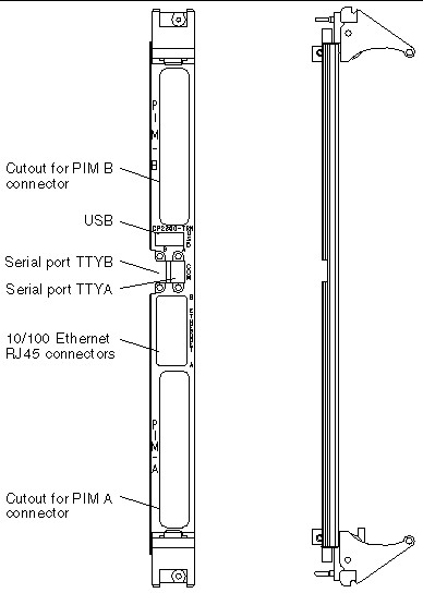
FIGURE 4-13 shows the ports on the rear transition card for the Netra CP2300 board.
FIGURE 4-13 Rear Transition Card for the Netra CP2300 Board
 [ D ]
[ D ]
Following are figures and tables showing the pinouts for each of the ports on the rear transition card for the Netra CP2300 board:
PIM Connectors
PIM A has two 64-pin connectors at J4 and J5, and PIM B has two 64-pin connectors at J6 and J7. See FIGURE 4-14 for the connector pin numbering, and see FIGURE 4-13 for the location of these connectors on the transition card.
FIGURE 4-14 PIM Connector Pins

PIM A Connector Pin Assignments
The PIM A connector is switch selectable with the EIDE connector. On the back of the Netra CP2300 cPSB board, there are three DIP switches: SW501, SW502, and SW503. When all of the positions on SW501 and SW502, and positions 1 through 9 on SW503 are set to Off, the EIDE connector is disabled and all of the PIM A connector pins are available. When these switch positions are off, the EIDE connector is active and PIM A J5 connector I/0 pins 1 to 29 (signals PMC_A_IO_1 through PMC_A_IO_29) are disabled and must be disconnected.
Refer to the Netra CP2300 cPSB Board Installation and Technical Reference Manual (816-7186) for more information about switch settings.
TABLE 4-15 lists the pin assignments for the PIM A connector at J4, and TABLE 4-16 lists the pin assignments for the PIM A connector at J5.
TABLE 4-15 PIM A Connector J4
|
Signal Name
|
Pin
|
Pin
|
Signal Name
|
|
SMC_TX
|
1
|
2
|
+12V
|
|
SMC_RX
|
3
|
4
|
|
|
+5V
|
5
|
6
|
|
|
TXN_I2C_SDA
|
7
|
8
|
|
|
TXN_I2C_SCL
|
9
|
10
|
+3.3V
|
|
I2C_PWR
|
11
|
12
|
|
|
GND
|
13
|
14
|
|
|
|
15
|
16
|
|
|
|
17
|
18
|
GND
|
|
RSV(PCI_RST#)
|
19
|
20
|
|
|
+5V
|
21
|
22
|
|
|
RSV
|
23
|
24
|
|
|
RSV
|
25
|
26
|
+3.3V
|
|
|
27
|
28
|
|
|
GND
|
29
|
30
|
|
|
|
31
|
32
|
|
|
|
33
|
34
|
GND
|
|
|
35
|
36
|
|
|
+5V
|
37
|
38
|
|
|
|
39
|
40
|
|
|
|
41
|
42
|
+3.3V
|
|
|
43
|
44
|
|
|
GND
|
45
|
46
|
|
|
|
47
|
48
|
|
|
|
49
|
50
|
GND
|
|
|
51
|
52
|
|
|
+5V
|
53
|
54
|
|
|
|
55
|
56
|
|
|
|
57
|
58
|
+3.3V
|
|
|
59
|
60
|
|
|
-12V
|
61
|
62
|
|
|
|
63
|
64
|
|
TABLE 4-16 PIM A Connector J5
|
Signal Name
|
Pin
|
Pin
|
Signal Name
|
|
PMC_A_IO_1
|
1
|
2
|
PMC_A_IO_2
|
|
PMC_A_IO_3
|
3
|
4
|
PMC_A_IO_4
|
|
PMC_A_IO_5
|
5
|
6
|
PMC_A_IO_6
|
|
PMC_A_IO_7
|
7
|
8
|
PMC_A_IO_8
|
|
PMC_A_IO_9
|
9
|
10
|
PMC_A_IO_10
|
|
PMC_A_IO_11
|
11
|
12
|
PMC_A_IO_12
|
|
PMC_A_IO_13
|
13
|
14
|
PMC_A_IO_14
|
|
PMC_A_IO_15
|
15
|
16
|
PMC_A_IO_16
|
|
PMC_A_IO_17
|
17
|
18
|
PMC_A_IO_18
|
|
PMC_A_IO_19
|
19
|
20
|
PMC_A_IO_20
|
|
PMC_A_IO_21
|
21
|
22
|
PMC_A_IO_22
|
|
PMC_A_IO_23
|
23
|
24
|
PMC_A_IO_24
|
|
PMC_A_IO_25
|
25
|
26
|
PMC_A_IO_26
|
|
PMC_A_IO_27
|
27
|
28
|
PMC_A_IO_28
|
|
PMC_A_IO_29
|
29
|
30
|
PMC_A_IO_30
|
|
PMC_A_IO_31
|
31
|
32
|
PMC_A_IO_32
|
|
PMC_A_IO_33
|
33
|
34
|
PMC_A_IO_34
|
|
PMC_A_IO_35
|
35
|
36
|
PMC_A_IO_36
|
|
PMC_A_IO_37
|
37
|
38
|
PMC_A_IO_38
|
|
PMC_A_IO_39
|
39
|
40
|
PMC_A_IO_40
|
|
PMC_A_IO_41
|
41
|
42
|
PMC_A_IO_42
|
|
PMC_A_IO_43
|
43
|
44
|
PMC_A_IO_44
|
|
PMC_A_IO_45
|
45
|
46
|
PMC_A_IO_46
|
|
PMC_A_IO_47
|
47
|
48
|
PMC_A_IO_48
|
|
PMC_A_IO_49
|
49
|
50
|
PMC_A_IO_50
|
|
PMC_A_IO_51
|
51
|
52
|
PMC_A_IO_52
|
|
PMC_A_IO_53
|
53
|
54
|
PMC_A_IO_54
|
|
PMC_A_IO_55
|
55
|
56
|
PMC_A_IO_56
|
|
PMC_A_IO_57
|
57
|
58
|
PMC_A_IO_58
|
|
PMC_A_IO_59
|
59
|
60
|
PMC_A_IO_60
|
|
PMC_A_IO_61
|
61
|
62
|
PMC_A_IO_62
|
|
PMC_A_IO_63
|
63
|
64
|
PMC_A_IO_64
|
PIM B Connector Pin Assignments
TABLE 4-17 lists the pin assignments for the PIM B connector at J6, and TABLE 4-18 lists the pin assignments for the PIM B connector at J7.
TABLE 4-17 PIM B Connector J6
|
Signal Name
|
Pin
|
Pin
|
Signal Name
|
|
SMC_TX
|
1
|
2
|
+12V
|
|
SMC_RX
|
3
|
4
|
|
|
+5V
|
5
|
6
|
|
|
TXN_I2C_SDA
|
7
|
8
|
|
|
TXN_I2C_SCL
|
9
|
10
|
+3.3V
|
|
I2C_PWR
|
11
|
12
|
|
|
GND
|
13
|
14
|
|
|
|
15
|
16
|
|
|
|
17
|
18
|
GND
|
|
RSV(PCI_RST#)
|
19
|
20
|
|
|
+5V
|
21
|
22
|
|
|
RSV
|
23
|
24
|
|
|
RSV
|
25
|
26
|
+3.3V
|
|
|
27
|
28
|
|
|
GND
|
29
|
30
|
|
|
|
31
|
32
|
|
|
|
33
|
34
|
GND
|
|
|
35
|
36
|
|
|
+5V
|
37
|
38
|
|
|
|
39
|
40
|
|
|
|
41
|
42
|
+3.3V
|
|
|
43
|
44
|
|
|
GND
|
45
|
46
|
|
|
|
47
|
48
|
|
|
|
49
|
50
|
GND
|
|
|
51
|
52
|
|
|
+5V
|
53
|
54
|
|
|
|
55
|
56
|
|
|
|
57
|
58
|
+3.3V
|
|
|
59
|
60
|
|
|
-12V
|
61
|
62
|
|
|
|
63
|
64
|
|
TABLE 4-18 PIM B Connector J7
|
Signal Name
|
Pin
|
Pin
|
Signal Name
|
|
PMC_B_IO_1
|
1
|
2
|
PMC_B_IO_2
|
|
PMC_B_IO_3
|
3
|
4
|
PMC_B_IO_4
|
|
PMC_B_IO_5
|
5
|
6
|
PMC_B_IO_6
|
|
PMC_B_IO_7
|
7
|
8
|
PMC_B_IO_8
|
|
PMC_B_IO_9
|
9
|
10
|
PMC_B_IO_10
|
|
PMC_B_IO_11
|
11
|
12
|
PMC_B_IO_12
|
|
PMC_B_IO_13
|
13
|
14
|
PMC_B_IO_14
|
|
PMC_B_IO_15
|
15
|
16
|
PMC_B_IO_16
|
|
PMC_B_IO_17
|
17
|
18
|
PMC_B_IO_18
|
|
PMC_B_IO_19
|
19
|
20
|
PMC_B_IO_20
|
|
PMC_B_IO_21
|
21
|
22
|
PMC_B_IO_22
|
|
PMC_B_IO_23
|
23
|
24
|
PMC_B_IO_24
|
|
PMC_B_IO_25
|
25
|
26
|
PMC_B_IO_26
|
|
PMC_B_IO_27
|
27
|
28
|
PMC_B_IO_28
|
|
PMC_B_IO_29
|
29
|
30
|
PMC_B_IO_30
|
|
PMC_B_IO_31
|
31
|
32
|
PMC_B_IO_32
|
|
PMC_B_IO_33
|
33
|
34
|
PMC_B_IO_34
|
|
PMC_B_IO_35
|
35
|
36
|
PMC_B_IO_36
|
|
PMC_B_IO_37
|
37
|
38
|
PMC_B_IO_38
|
|
PMC_B_IO_39
|
39
|
40
|
PMC_B_IO_40
|
|
PMC_B_IO_41
|
41
|
42
|
PMC_B_IO_42
|
|
PMC_B_IO_43
|
43
|
44
|
PMC_B_IO_44
|
|
PMC_B_IO_45
|
45
|
46
|
PMC_B_IO_46
|
|
PMC_B_IO_47
|
47
|
48
|
PMC_B_IO_48
|
|
PMC_B_IO_49
|
49
|
50
|
PMC_B_IO_50
|
|
PMC_B_IO_51
|
51
|
52
|
PMC_B_IO_52
|
|
PMC_B_IO_53
|
53
|
54
|
PMC_B_IO_54
|
|
PMC_B_IO_55
|
55
|
56
|
PMC_B_IO_56
|
|
PMC_B_IO_57
|
57
|
58
|
PMC_B_IO_58
|
|
PMC_B_IO_59
|
59
|
60
|
PMC_B_IO_60
|
|
PMC_B_IO_61
|
61
|
62
|
PMC_B_IO_62
|
|
PMC_B_IO_63
|
63
|
64
|
PMC_B_IO_64
|
USB Port
FIGURE 4-15 shows the USB connector port A on the rear transition card for the Netra CP2300 board. TABLE 4-19 lists the pin assignments for the USB port.
FIGURE 4-15 USB Connector Port A Pins

TABLE 4-19 USB Port A
|
Pin
|
Signal
|
|
1
|
+5V POWER
|
|
2
|
POS
|
|
3
|
NEG
|
|
4
|
GND
|
Serial Ports
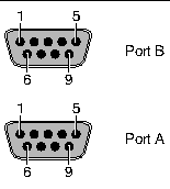
Two serial ports from the Netra CP2300 transition card are available through the rear panel with single-stacked, 9-pin connectors. One connector is assigned to Port A and the other connector to Port B (FIGURE 4-16).
FIGURE 4-16 Serial Port Connector Pins

The signal interfaces of the connectors are described in TABLE 4-20 and TABLE 4-21.
TABLE 4-20 Serial Port A
|
Pin No.
|
Signal
|
Pin No.
|
Signal
|
|
1
|
SER_A_DCD
|
6
|
SER_A_DSR
|
|
2
|
SER_A_RXD
|
7
|
SER_A_RTS
|
|
3
|
SER_A_TXD
|
8
|
SER_A_CTS
|
|
4
|
SER_A_DTR
|
9
|
SER_A_RI
|
|
5
|
GND_A
|
|
|
TABLE 4-21 Serial Port B
|
Pin No.
|
Signal
|
Pin No.
|
Signal
|
|
1
|
SER_B_DCD
|
6
|
SER_B_DSR
|
|
2
|
SER_B_RXD
|
7
|
SER_B_RTS
|
|
3
|
SER_B_TXD
|
8
|
SER_B_CTS
|
|
4
|
SER_B_DTR
|
9
|
SER_B_RI
|
|
5
|
GND_B
|
|
|
Fast Ethernet Connectors
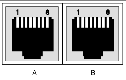
The dual-jack RJ-45 (J701) AMP1116353-8 Ethernet connectors, located on the transition card's back panel, provide two 10/100 Mbit/sec fast Ethernet ports.
FIGURE 4-17 Fast Ethernet Connector Pins

By default, the Netra CP2300 board is set so that Ethernet traffic is routed to the switching fabric board rear transition card, and the fast Ethernet connectors on the Netra CP2300 rear transition card are disabled. You can use the fast Ethernet connectors on the Netra CP2300 rear transition card only if you changed the default settings on the Netra CP2300 board beforehand. Refer to Ethernet Networking on the Netra CP2300 Board for more information before proceeding with these instructions.


 [ D ]
[ D ]


 [ D ]
[ D ]


 [ D ]
[ D ]


