Specification and Connectors
|
This appendix provides the specifications and connector pin-outs for the
Netra CP2300 transition card.
Specifications
This section provides mechanical, electrical, environmental, and other relevant specifications for the Netra CP2300 transition card.
Physical Dimensions
TABLE A-1 shows the physical dimensions for the Netra CP2300 transition card.
TABLE A-1 Physical Dimensions
|
Board Specifications
|
Dimensions
|
|
Form Factor
|
6U
|
|
Length
|
233.20 mm (9.18 inches)
|
|
Width
|
79.85 mm (3.14 inches)
|
|
Height
|
20.02 mm (0.79 inches)
|
Power Requirements
The Netra CP2300 transition card has mainly passive components. However, some power from the backplane is provided to PIM carriers A and B and to the I2C EEPROM.
For information on PIM allowable dissipation and limits on PIM power consumption, refer to the VITA 36, PMC I/O Module Standard.
Electrical Requirements
The Netra CP2300 transition card is powered through the Netra CP2300 cPSB board. The Netra CP2300 cPSB board provides the following voltages: 3.3V/5V/12V/-12V (total combined maximum voltage: 2.5 W).
The Netra CP2300 transition card has mainly passive components. However, some power is provided from the chassis backplane to the I2C EEPROM and PIM carriers. For more information, see the Netra CP2300 cPSB Board Installation and Technical Reference Manual (816-7186-xx).
Environmental Specification and Compliance
For details on the environmental specifications and compliance, please refer to the Important Safety Information for Sun Hardware Systems (816-7190-10) and the Netra CP2300 cPSB Board Installation and Technical Reference Manual (816-7186-xx) documents.
You can download and view these documents from the following web site:
http://www.sun.com/documentation
ConnectorsTransition Card I/O Face Plate Connectors
This section lists the pins and signal names of the I/O faceplate connectors on the transition card.
USB Port
USB connector port A is available on the Netra CP2300 transition card I/O panel.
FIGURE A-1 USB Connector Port A Pins

TABLE A-2 Universal Serial Bus Port A
|
Pin
|
Signal
|
|
1
|
+5V POWER
|
|
2
|
POS
|
|
3
|
NEG
|
|
4
|
GND
|
Serial Ports
Two serial ports from the Netra CP2300 transition card are available through the rear panel with single-stacked, 9-pin connectors. One connector is assigned to Port A and the other connector to Port B (FIGURE A-2).
FIGURE A-2 Serial Port Connector Pins
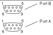
The signal interface of the connectors are described in the following two tables.
TABLE A-3 Serial Port A
|
Pin
|
Signal
|
|
1
|
SER_A_DCD
|
|
2
|
SER_A_RXD
|
|
3
|
SER_A_TXD
|
|
4
|
SER_A_DTR
|
|
5
|
GND_A
|
|
6
|
SER_A_DSR
|
|
7
|
SER_A_RTS
|
|
8
|
SER_A_CTS
|
|
9
|
SER_A_RI
|
TABLE A-4 Serial Port B
|
Pin
|
Signal
|
|
1
|
SER_B_DCD
|
|
2
|
SER_B_RXD
|
|
3
|
SER_B_TXD
|
|
4
|
SER_B_DTR
|
|
5
|
GND_B
|
|
6
|
SER_B_DSR
|
|
7
|
SER_B_RTS
|
|
8
|
SER_B_CTS
|
|
9
|
SER_B_RI
|
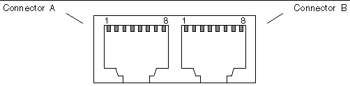
Fast Ethernet Connectors
The dual-jack RJ45 AMP1116353-8 Ethernet connectors, located on the transition card's back panel, provide two 10/100 Mbps fast Ethernet ports.
FIGURE A-3 Fast Ethernet Connector Pins
By default, these Ethernet ports are not available if the Netra CP2300 cPSB board is set to use the chassis's packet-switched backplane (PSB) Ethernet network. In order to use the transition card's Ethernet connectors, you must set the 0 position of the Netra CP2300 board SW503 DIP switch on (see FIGURE A-4). After setting this DIP switch to on, the PSB Ethernet network will not be available, but you will be able to use the transition card's two RJ45 connectors.
FIGURE A-4 Setting the SW503 DIP Switch on the Netra CP2300 cPSB Board
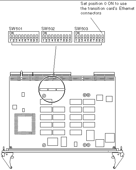
TABLE A-5 lists the pin assignments for the dual-jack RJ45 AMP1116353-8 Fast Ethernet connectors.
TABLE A-5 Fast Ethernet Ports A and B
|
Ethernet Port A
|
Ethernet Port B
|
|
Pin
|
Signal
|
Pin
|
Signal
|
|
1
|
NET2_TX_P through magnetics
|
1
|
NET2_TX_P through magnetics
|
|
2
|
NET2_TX_N through magnetics
|
2
|
NET2_TX_N through magnetics
|
|
3
|
NET2_RX_P through magnetics
|
3
|
NET2_RX_P through magnetics
|
|
4
|
|
4
|
|
|
5
|
|
5
|
|
|
6
|
NET2_RX_N through magnetics
|
6
|
NET2_RX_N through magnetics
|
|
7
|
|
7
|
|
|
8
|
|
8
|
|
On-Board Interfaces and Connectors on the Netra CP2300 Transition Card
FIGURE A-5 shows the on-board interfaces and connectors on the transition card. The numbers in parentheses display how the interfaces are labeled on the transition card.
.
FIGURE A-5 Netra CP2300 Transition Card On-Board Connectors and Interfaces
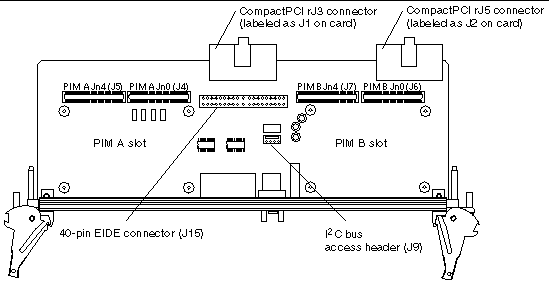
I2C Serial Bus Access Header
The I2C serial bus is routed onto the Netra CP2300 RTM through the rJ5 backplane connector (which is labeled as J2 on the transition card). The Netra CP2300 transition card I2C bus supports one I2C function--provide information about itself through nonvolatile memory. FIGURE A-6 shows the I2C serial bus access header and TABLE A-6 lists the pin assignments.
FIGURE A-6 I2C Serial Bus Access Header Pins

TABLE A-6 I2C Serial Bus Access Header Pin Assignments
|
Pin
|
Signal
|
|
1
|
I2C_PWR
|
|
2
|
TXN_I2C_SDA (Data/Address)
|
|
3
|
TXN_I2C_SCL (Clock)
|
|
4
|
GND
|
PIM Connectors
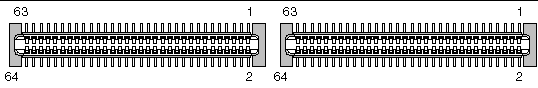
The PIM A slot has two 64-pin connectors: PIM A Jn4 (labeled J5 on the transition card) and PIM A Jn0 (J4). The PIM B slot has two 64-pin connectors: PIM B Jn4 (J7) and PIM B Jn0 (J6). See FIGURE A-7 for the connector pin numbering, and see FIGURE A-5 for the location of these connectors on the transition card.
FIGURE A-7 PIM Connector Pins
PIM A Connector Pin Assignments
The PIM A connector is switch-selectable with the EIDE connector. On the back of the Netra CP2300 cPSB board, there are three DIP switches: SW501, SW502, and SW503 (see FIGURE A-4 for the location of these switches). When all of the positions on SW501 and SW502, and positions 1 through 9 on SW503 are set to OFF, the EIDE connector is disabled and all of the PIM A connector pins are available. When these switch positions are set to ON, the EIDE connector is active and PIM A Jn4 (labeled as J5) connector I/0 pins 1 to 29 (signals PMC_A_IO_1 through PMC_A_IO_29) are disabled and must be disconnected.
Refer to the Netra CP2300 cPSB Board Installation and Technical Reference Manual
(816-7186-xx) for more information about DIP switch settings.
TABLE A-7 lists the pin assignments for the PIM A Jn0 (J4) connector, and TABLE A-8 lists the pin assignments for the PIM A Jn4 (J5) connector.
TABLE A-7 PIM A Jn0 Connector (J4)
|
Signal Name
|
Pin
|
Pin
|
Signal Name
|
|
SMC_TX
|
1
|
2
|
+12V
|
|
SMC_RX
|
3
|
4
|
|
|
+5V
|
5
|
6
|
|
|
TXN_I2C_SDA
|
7
|
8
|
|
|
TXN_I2C_SCL
|
9
|
10
|
+3.3V
|
|
I2C_PWR
|
11
|
12
|
|
|
GND
|
13
|
14
|
|
|
|
15
|
16
|
|
|
|
17
|
18
|
GND
|
|
RSV(PCI_RST#)
|
19
|
20
|
|
|
+5V
|
21
|
22
|
|
|
RSV
|
23
|
24
|
|
|
RSV
|
25
|
26
|
+3.3V
|
|
|
27
|
28
|
|
|
GND
|
29
|
30
|
|
|
|
31
|
32
|
|
|
|
33
|
34
|
GND
|
|
|
35
|
36
|
|
|
+5V
|
37
|
38
|
|
|
|
39
|
40
|
|
|
|
41
|
42
|
+3.3V
|
|
|
43
|
44
|
|
|
GND
|
45
|
46
|
|
|
|
47
|
48
|
|
|
|
49
|
50
|
GND
|
|
|
51
|
52
|
|
|
+5V
|
53
|
54
|
|
|
|
55
|
56
|
|
|
|
57
|
58
|
+3.3V
|
|
|
59
|
60
|
|
|
-12V
|
61
|
62
|
|
|
|
63
|
64
|
|
TABLE A-8 PIM A Jn4 Connector (J5)
|
Signal Name
|
Pin
|
Pin
|
Signal Name
|
|
PMC_A_IO_1
|
1
|
2
|
PMC_A_IO_2
|
|
PMC_A_IO_3
|
3
|
4
|
PMC_A_IO_4
|
|
PMC_A_IO_5
|
5
|
6
|
PMC_A_IO_6
|
|
PMC_A_IO_7
|
7
|
8
|
PMC_A_IO_8
|
|
PMC_A_IO_9
|
9
|
10
|
PMC_A_IO_10
|
|
PMC_A_IO_11
|
11
|
12
|
PMC_A_IO_12
|
|
PMC_A_IO_13
|
13
|
14
|
PMC_A_IO_14
|
|
PMC_A_IO_15
|
15
|
16
|
PMC_A_IO_16
|
|
PMC_A_IO_17
|
17
|
18
|
PMC_A_IO_18
|
|
PMC_A_IO_19
|
19
|
20
|
PMC_A_IO_20
|
|
PMC_A_IO_21
|
21
|
22
|
PMC_A_IO_22
|
|
PMC_A_IO_23
|
23
|
24
|
PMC_A_IO_24
|
|
PMC_A_IO_25
|
25
|
26
|
PMC_A_IO_26
|
|
PMC_A_IO_27
|
27
|
28
|
PMC_A_IO_28
|
|
PMC_A_IO_29
|
29
|
30
|
PMC_A_IO_30
|
|
PMC_A_IO_31
|
31
|
32
|
PMC_A_IO_32
|
|
PMC_A_IO_33
|
33
|
34
|
PMC_A_IO_34
|
|
PMC_A_IO_35
|
35
|
36
|
PMC_A_IO_36
|
|
PMC_A_IO_37
|
37
|
38
|
PMC_A_IO_38
|
|
PMC_A_IO_39
|
39
|
40
|
PMC_A_IO_40
|
|
PMC_A_IO_41
|
41
|
42
|
PMC_A_IO_42
|
|
PMC_A_IO_43
|
43
|
44
|
PMC_A_IO_44
|
|
PMC_A_IO_45
|
45
|
46
|
PMC_A_IO_46
|
|
PMC_A_IO_47
|
47
|
48
|
PMC_A_IO_48
|
|
PMC_A_IO_49
|
49
|
50
|
PMC_A_IO_50
|
|
PMC_A_IO_51
|
51
|
52
|
PMC_A_IO_52
|
|
PMC_A_IO_53
|
53
|
54
|
PMC_A_IO_54
|
|
PMC_A_IO_55
|
55
|
56
|
PMC_A_IO_56
|
|
PMC_A_IO_57
|
57
|
58
|
PMC_A_IO_58
|
|
PMC_A_IO_59
|
59
|
60
|
PMC_A_IO_60
|
|
PMC_A_IO_61
|
61
|
62
|
PMC_A_IO_62
|
|
PMC_A_IO_63
|
63
|
64
|
PMC_A_IO_64
|
PIM B Connector Pin Assignments
TABLE A-9 lists the pin assignments for the PIM B Jn0 (J6) connector, and TABLE A-10 lists the pin assignments for the PIM B Jn4 (J7) connector.
TABLE A-9 PIM B Jn0 Connector (J6)
|
Signal Name
|
Pin
|
Pin
|
Signal Name
|
|
SMC_TX
|
1
|
2
|
+12V
|
|
SMC_RX
|
3
|
4
|
|
|
+5V
|
5
|
6
|
|
|
TXN_I2C_SDA
|
7
|
8
|
|
|
TXN_I2C_SCL
|
9
|
10
|
+3.3V
|
|
I2C_PWR
|
11
|
12
|
|
|
GND
|
13
|
14
|
|
|
|
15
|
16
|
|
|
|
17
|
18
|
GND
|
|
RSV(PCI_RST#)
|
19
|
20
|
|
|
+5V
|
21
|
22
|
|
|
RSV
|
23
|
24
|
|
|
RSV
|
25
|
26
|
+3.3V
|
|
|
27
|
28
|
|
|
GND
|
29
|
30
|
|
|
|
31
|
32
|
|
|
|
33
|
34
|
GND
|
|
|
35
|
36
|
|
|
+5V
|
37
|
38
|
|
|
|
39
|
40
|
|
|
|
41
|
42
|
+3.3V
|
|
|
43
|
44
|
|
|
GND
|
45
|
46
|
|
|
|
47
|
48
|
|
|
|
49
|
50
|
GND
|
|
|
51
|
52
|
|
|
+5V
|
53
|
54
|
|
|
|
55
|
56
|
|
|
|
57
|
58
|
+3.3V
|
|
|
59
|
60
|
|
|
-12V
|
61
|
62
|
|
|
|
63
|
64
|
|
TABLE A-10 PIM B Jn4 Connector (J7)
|
Signal Name
|
Pin
|
Pin
|
Signal Name
|
|
PMC_B_IO_1
|
1
|
2
|
PMC_B_IO_2
|
|
PMC_B_IO_3
|
3
|
4
|
PMC_B_IO_4
|
|
PMC_B_IO_5
|
5
|
6
|
PMC_B_IO_6
|
|
PMC_B_IO_7
|
7
|
8
|
PMC_B_IO_8
|
|
PMC_B_IO_9
|
9
|
10
|
PMC_B_IO_10
|
|
PMC_B_IO_11
|
11
|
12
|
PMC_B_IO_12
|
|
PMC_B_IO_13
|
13
|
14
|
PMC_B_IO_14
|
|
PMC_B_IO_15
|
15
|
16
|
PMC_B_IO_16
|
|
PMC_B_IO_17
|
17
|
18
|
PMC_B_IO_18
|
|
PMC_B_IO_19
|
19
|
20
|
PMC_B_IO_20
|
|
PMC_B_IO_21
|
21
|
22
|
PMC_B_IO_22
|
|
PMC_B_IO_23
|
23
|
24
|
PMC_B_IO_24
|
|
PMC_B_IO_25
|
25
|
26
|
PMC_B_IO_26
|
|
PMC_B_IO_27
|
27
|
28
|
PMC_B_IO_28
|
|
PMC_B_IO_29
|
29
|
30
|
PMC_B_IO_30
|
|
PMC_B_IO_31
|
31
|
32
|
PMC_B_IO_32
|
|
PMC_B_IO_33
|
33
|
34
|
PMC_B_IO_34
|
|
PMC_B_IO_35
|
35
|
36
|
PMC_B_IO_36
|
|
PMC_B_IO_37
|
37
|
38
|
PMC_B_IO_38
|
|
PMC_B_IO_39
|
39
|
40
|
PMC_B_IO_40
|
|
PMC_B_IO_41
|
41
|
42
|
PMC_B_IO_42
|
|
PMC_B_IO_43
|
43
|
44
|
PMC_B_IO_44
|
|
PMC_B_IO_45
|
45
|
46
|
PMC_B_IO_46
|
|
PMC_B_IO_47
|
47
|
48
|
PMC_B_IO_48
|
|
PMC_B_IO_49
|
49
|
50
|
PMC_B_IO_50
|
|
PMC_B_IO_51
|
51
|
52
|
PMC_B_IO_52
|
|
PMC_B_IO_53
|
53
|
54
|
PMC_B_IO_54
|
|
PMC_B_IO_55
|
55
|
56
|
PMC_B_IO_56
|
|
PMC_B_IO_57
|
57
|
58
|
PMC_B_IO_58
|
|
PMC_B_IO_59
|
59
|
60
|
PMC_B_IO_60
|
|
PMC_B_IO_61
|
61
|
62
|
PMC_B_IO_62
|
|
PMC_B_IO_63
|
63
|
64
|
PMC_B_IO_64
|
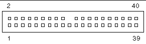
EIDE Connector
The single EIDE bus is brought onto the transition card from the Netra CP2300 board through the rJ3 backplane connector (which is labeled as J1 on the transition card). The EIDE bus is routed to a 40-pin EIDE connector header.
FIGURE A-8 EIDE Connector Pins
The EIDE bus is mutually exclusive with the PIM A Jn4 (J5) connector I/O pins 1-29. By setting DIP switches on the Netra CP2300 board, you can select the EIDE bus or the PIM A Jn4 (J5) connector signals PIM_A_IO_1 through PIM_A_IO_29.
On the solder-side of the Netra CP2300 cPSB board, there are three DIP switches: SW501, SW502, and SW503 (see FIGURE A-4 for the location of these switches). When all of the positions on SW501 and SW502, and positions 1 through 9 on SW503 are set to OFF, the EIDE connector is disabled and all of the PIM A connector pins are available. When these switch positions are set to ON, the EIDE connector is active and PIM A Jn4 (J5) connector I/0 pins 1 to 29 (signals PMC_A_IO_1 through PMC_A_IO_29) are disabled and must be disconnected (see TABLE A-8).
Refer to the Netra CP2300 cPSB Board Installation and Technical Reference Manual
(816-7186-xx) for more information about switch settings.
TABLE A-11 lists the mutually exclusive 40-pin EIDE connector and the Netra CP2300 board CompactPCI rJ3 (J1) PIM A I/O pin assignments.
TABLE A-11 EIDE Connector Pin Assignments
|
rJ3 Signal
|
Header Signal
|
PIN
|
PIN
|
Header Signal
|
rJ3 Signal
|
|
PMC_A_IO_17
|
IDE_RST#
|
1
|
2
|
GND
|
|
|
PMC_A_IO_8
|
IDE_D7
|
3
|
4
|
IDE_D8
|
PMC_A_IO_9
|
|
PMC_A_IO_7
|
IDE_D6
|
5
|
6
|
IDE_D9
|
PMC_A_IO_10
|
|
PMC_A_IO_6
|
IDE_D5
|
7
|
8
|
IDE_D10
|
PMC_A_IO_11
|
|
PMC_A_IO_5
|
IDE_D4
|
9
|
10
|
IDE_D11
|
PMC_A_IO_12
|
|
PMC_A_IO_4
|
IDE_D3
|
11
|
12
|
IDE_D12
|
PMC_A_IO_13
|
|
PMC_A_IO_3
|
IDE_D2
|
13
|
14
|
IDE_D13
|
PMC_A_IO_14
|
|
PMC_A_IO_2
|
IDE_D1
|
15
|
16
|
IDE_D14
|
PMC_A_IO_15
|
|
PMC_A_IO_1
|
IDE_D0
|
17
|
18
|
IDE_D15
|
PMC_A_IO_16
|
|
|
GND
|
19
|
20
|
NC
|
|
|
PMC_A_IO_26
|
IDE_DRQ
|
21
|
22
|
GND
|
|
|
PMC_A_IO_18
|
IDE_IOW
|
23
|
24
|
GND
|
|
|
PMC_A_IO_19
|
IDE_IOR
|
25
|
26
|
GND
|
|
|
PMC_A_IO_28
|
IDE_IORDY
|
27
|
28
|
RES to GND
|
|
|
PMC_A_IO_25
|
IDE_ACK
|
29
|
30
|
GND
|
|
|
PMC_A_IO_27
|
IDE_IRQ
|
31
|
32
|
NC
|
|
|
PMC_A_IO_20
|
IDE_A1
|
33
|
34
|
C0_CBLID
|
PMC_A_IO_29
|
|
PMC_A_IO_21
|
IDE_A0
|
35
|
36
|
IDE_A2
|
PMC_A_IO_22
|
|
PMC_A_IO_23
|
IDE_CS1#
|
37
|
38
|
IDE_CS3#
|
PMC_A_IO_24
|
|
|
NC
|
39
|
40
|
GND
|
|
Backplane Interfaces
The Netra CP2300 transition card interfaces to the cPSB bus through the CompactPCI rJ3 (labeled as J1 on the transition card) and rJ5 (J2) backplane connectors. The pin assignments for these two sets of connectors are provided in this section.
CompactPCI rJ3 Connector (J1)
TABLE A-12 shows the pin assignments for the CompactPCI rJ3 connector. This connector is labeled J1 on the transition card (see FIGURE A-5 for the location).
FIGURE A-9 CompactPCI rJ3 Connector (J1) Pins
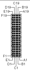
TABLE A-12 CompactPCI rJ3 Connector (J1) Pin Assignments
|
Pin #
|
Row A
|
Row B
|
Row C
|
Row D
|
Row E
|
|
19
|
RESERVE
|
RESERVE
|
RESERVE
|
RESERVE
|
GND
|
|
18
|
PSB_A_TX_POS
|
PSB_A_TX_NEG
|
GND
|
NC
|
NC
|
|
17
|
PSB_A_RX_POS
|
PSB_A_RX_NEG
|
GND
|
NC
|
NC
|
|
16
|
PSB_B_TX_POS
|
PSB_B_TX_NEG
|
GND
|
NC
|
NC
|
|
15
|
PSB_B_RX_POS
|
PSB_B_RX_NEG
|
GND
|
NC
|
NC
|
|
14
|
+3.3V
|
+3.3V
|
+3.3V
|
+5V
|
+5V
|
|
13
|
PMC_A_IO_5
|
PMC_A_IO_4
|
PMC_A_IO_3
|
PMC_A_IO_2
|
PMC_A_IO_1
|
|
12
|
PMC_A_IO_10
|
PMC_A_IO_9
|
PMC_A_IO_8
|
PMC_A_IO_7
|
PMC_A_IO_6
|
|
11
|
PMC_A_IO_15
|
PMC_A_IO_14
|
PMC_A_IO_13
|
PMC_A_IO_12
|
PMC_A_IO_11
|
|
10
|
PMC_A_IO_20
|
PMC_A_IO_19
|
PMC_A_IO_18
|
PMC_A_IO_17
|
PMC_A_IO_16
|
|
9
|
PMC_A_IO_25
|
PMC_A_IO_24
|
PMC_A_IO_23
|
PMC_A_IO_22
|
PMC_A_IO_21
|
|
8
|
PMC_A_IO_30
|
PMC_A_IO_29
|
PMC_A_IO_28
|
PMC_A_IO_27
|
PMC_A_IO_26
|
|
7
|
PMC_A_IO_35
|
PMC_A_IO_34
|
PMC_A_IO_33
|
PMC_A_IO_32
|
PMC_A_IO_31
|
|
6
|
PMC_A_IO_40
|
PMC_A_IO_39
|
PMC_A_IO_38
|
PMC_A_IO_37
|
PMC_A_IO_36
|
|
5
|
PMC_A_IO_45
|
PMC_A_IO_44
|
PMC_A_IO_43
|
PMC_A_IO_42
|
PMC_A_IO_41
|
|
4
|
PMC_A_IO_50
|
PMC_A_IO_49
|
PMC_A_IO_48
|
PMC_A_IO_47
|
PMC_A_IO_46
|
|
3
|
PMC_A_IO_55
|
PMC_A_IO_54
|
PMC_A_IO_53
|
PMC_A_IO_52
|
PMC_A_IO_51
|
|
2
|
PMC_A_IO_60
|
PMC_A_IO_59
|
PMC_A_IO_58
|
PMC_A_IO_57
|
PMC_A_IO_56
|
|
1
|
+5V
|
PMC_A_IO_64
|
PMC_A_IO_63
|
PMC_A_IO_62
|
PMC_A_IO_61
|
|
Note - The pin assignments for every pin in rows F and Z are ground.
|
CompactPCI rJ5 Connector (J2)
TABLE A-13 shows the pin assignments for the CompactPCI rJ5 connector. This connector is labeled J2 on the transition card (see FIGURE A-5 for the location).
FIGURE A-10 CompactPCI rJ5 Connector (J2) Pins
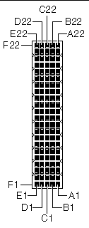
TABLE A-13 CompactPCI rJ5 Connector (J2) Pin Assignments
|
Pin #
|
Row A
|
Row B
|
Row C
|
Row D
|
Row E
|
|
22
|
PMC_B_IO_5
|
PMC_B_IO_4
|
PMC_B_IO_3
|
PMC_B_IO_2
|
PMC_B_IO_1
|
|
21
|
PMC_B_IO_10
|
PMC_B_IO_9
|
PMC_B_IO_8
|
PMC_B_IO_7
|
PMC_B_IO_6
|
|
20
|
PMC_B_IO_15
|
PMC_B_IO_14
|
PMC_B_IO_13
|
PMC_B_IO_12
|
PMC_B_IO_11
|
|
19
|
PMC_B_IO_20
|
PMC_B_IO_19
|
PMC_B_IO_18
|
PMC_B_IO_17
|
PMC_B_IO_16
|
|
18
|
PMC_B_IO_25
|
PMC_B_IO_24
|
PMC_B_IO_23
|
PMC_B_IO_22
|
PMC_B_IO_21
|
|
17
|
PMC_B_IO_30
|
PMC_B_IO_29
|
PMC_B_IO_28
|
PMC_B_IO_27
|
PMC_B_IO_26
|
|
16
|
PMC_B_IO_35
|
PMC_B_IO_34
|
PMC_B_IO_33
|
PMC_B_IO_32
|
PMC_B_IO_31
|
|
15
|
PMC_B_IO_40
|
PMC_B_IO_39
|
PMC_B_IO_38
|
PMC_B_IO_37
|
PMC_B_IO_36
|
|
14
|
PMC_B_IO_45
|
PMC_B_IO_44
|
PMC_B_IO_43
|
PMC_B_IO_42
|
PMC_B_IO_41
|
|
13
|
PMC_B_IO_50
|
PMC_B_IO_49
|
PMC_B_IO_48
|
PMC_B_IO_47
|
PMC_B_IO_46
|
|
12
|
PMC_B_IO_55
|
PMC_B_IO_54
|
PMC_B_IO_53
|
PMC_B_IO_52
|
PMC_B_IO_51
|
|
11
|
PMC_B_IO_60
|
PMC_B_IO_59
|
PMC_B_IO_58
|
PMC_B_IO_57
|
PMC_B_IO_56
|
|
10
|
RESERVE
|
PMC_B_IO_64
|
PMC_B_IO_63
|
PMC_B_IO_62
|
PMC_B_IO_61
|
|
9
|
SER_A_RTS
|
SER_A_DTR
|
SER_A_RI
|
GND
|
SER_A_CTS
|
|
8
|
SER_A_DCD
|
SER_A_TXD
|
SER_A_RXD
|
SER_A_DSR
|
+5V
|
|
7
|
SER_B_RTS
|
SER_B_DTR
|
SER_B_RI
|
SER_B_DSR
|
SER_B_CTS
|
|
6
|
SER_B_DCD
|
SER_B_TXD
|
SER_B_RXD
|
GND
|
GND
|
|
5
|
TXN_I2C_CLK
|
RESERVE
|
-12V
|
(NET2_RX_P)
|
(NET2_RX_N)
|
|
4
|
TXN_I2C_SDA
|
I2C_PWR
|
GND
|
(NET2_TX_P)
|
(NET2_TX_N)
|
|
3
|
(USB_B_POS)
|
(USB_B_NEG)
|
GND
|
GND
|
GND
|
|
2
|
USB_A_POS
|
USB_A_NEG
|
GND
|
(NET1_RX_P)
|
(NET1_RX_N)
|
|
1
|
GND
|
+3.3V
|
+12V
|
(NET1_TX_P)
|
(NET1_TX_N)
|
|
Note - The pin assignments for every pin in rows F and Z are ground.
|