| Netra CP2300 cPSB Board Installation and Technical Reference Manual
|
   
|
Connectors, Pinouts and Switch Settings
|
This chapter contains the following subsections:
|
Note - For pin assignments of the rear transition card connectors, refer to the transition card manual.
|
B.1 PMC Connectors
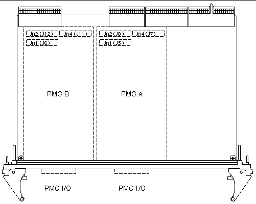
FIGURE B-1 shows the locations of PMC port connectors, and the tables below show contact allocations.
FIGURE B-1 Netra CP2300 Board PMC Port Connectors

|
Note - The P1386.1 standard reserves the Jn3 64-pin connector for PCI 64-bit extensions, so it is not fitted on the Netra CP2300 board.
|
TABLE B-1 lists how the PMC slot connectors are labelled on the board.
TABLE B-1 PMC Connector Labelling
|
PMC Slot
|
PMC Connector
|
Board Connector Label
|
|
PMC slot B
|
Jn1
|
J6
|
|
PMC slot B
|
Jn2
|
J12
|
|
PMC slot B
|
Jn4
|
J11
|
|
PMC slot A
|
Jn1
|
J5
|
|
PMC slot A
|
Jn2
|
J8
|
|
PMC slot A
|
Jn4
|
J7
|
B.1.1 PMC A Connector Interfaces
Corresponding to the Common Mezzanine Card (CMC) specification, the PMC A slot is comprised of three PMC connectors: Jn1 (labeled J5 on the board), Jn2 (J8), and Jn4 (J7). (The Jn3 connector is not fitted on the Netra CP2300 board.)
The following tables list the PMC A slot connector interfaces.
TABLE B-2 PMC A Jn1 (J5) Connector Interface
|
Pin
|
Description
|
Pin
|
Description
|
|
1
|
TCK; JTAG clock signal.
|
2
|
-12V
|
|
3
|
GND
|
4
|
PMC_A_INT_A_L
|
|
5
|
PMC_A_INT_B_L
|
6
|
PMC_A_INT_C_L
|
|
7
|
PMC_BUSMODE1_L
|
8
|
VCC (5V)
|
|
9
|
PMC_A_INT_D_L
|
10
|
NC
|
|
11
|
GND
|
12
|
NC
|
|
13
|
PMC_CLK
|
14
|
GND
|
|
15
|
GND
|
16
|
PMC_GNT_L
|
|
17
|
PMC_REQ_L
|
18
|
VCC
|
|
19
|
LOCAL_VIO
|
20
|
PCI_B_AD<31>
|
|
21
|
PCI_B_AD<28>
|
22
|
PCI_B_AD<27>
|
|
23
|
PCI_B_AD<25>
|
24
|
GND
|
|
25
|
GND
|
26
|
PCI_B_CBE3_L
|
|
27
|
PCI_B_AD<22>
|
28
|
PCI_B_AD<21>
|
|
29
|
PCI_B_AD<19>
|
30
|
VCC
|
|
31
|
LOCAL_VIO
|
32
|
PCI_B_AD<17>
|
|
33
|
PCI_B_FRAME_L
|
34
|
GND
|
|
35
|
GND
|
36
|
PCI_B_IRDY_L
|
|
37
|
PCI_B_DEVSEL_L
|
38
|
VCC
|
|
39
|
GND
|
40
|
PCI_B_LOCK_L
|
|
41
|
PMC_SDONE
|
42
|
PMC_SB0_L
|
|
43
|
PCI_B_PAR
|
44
|
GND
|
|
45
|
LOCAL_VIO
|
46
|
PCI_B_AD<15>
|
|
47
|
PCI_B_AD<12>
|
48
|
PCI_B_AD<11>
|
|
49
|
PCI_B_AD<9>
|
50
|
VCC
|
|
51
|
GND
|
52
|
PCI_B_CBE_L<0>
|
|
53
|
PCI_B_AD<6>
|
54
|
PCI_B_AD<5>
|
|
55
|
PCI_B_AD<4>
|
56
|
GND
|
|
57
|
LOCAL_VIO
|
58
|
PCI_B_AD<3>
|
|
59
|
PCI_B_AD<2>
|
60
|
PCI_B_AD<1>
|
|
61
|
PCI_B_AD<0>
|
62
|
VCC
|
|
63
|
GND
|
64
|
PCI_B_REQ64_L
|
TABLE B-3 PMC A Jn2 (J8) Connector Interface
|
Pin
|
Description
|
Pin
|
Description
|
|
1
|
+12V
|
2
|
JTAG_PMC_RST_L
|
|
3
|
TMS
|
4
|
PMC_TDO
|
|
5
|
PMC_TDI
|
6
|
GND
|
|
7
|
GND
|
8
|
NC
|
|
9
|
NC
|
10
|
NC
|
|
11
|
PMC_BUSMODE2_L
|
12
|
VDD (3.3V)
|
|
13
|
PCI_B_RST_L
|
14
|
PMC_BUSMODE3_L
|
|
15
|
VDD
|
16
|
PMC_BUSMODE4_L
|
|
17
|
NC
|
18
|
GND
|
|
19
|
PCI_B_AD<30>
|
20
|
PCI_B_AD<29>
|
|
21
|
GND
|
22
|
PCI_B_AD<26>
|
|
23
|
PCI_B_AD<24>
|
24
|
VDD
|
|
25
|
PCI_B_IDSEL
|
26
|
PCI_B_AD<23>
|
|
27
|
VDD
|
28
|
PCI_B_AD<20>
|
|
29
|
PCI_B_AD<18>
|
30
|
GND
|
|
31
|
PCI_B_AD<16>
|
32
|
PCI_B_CBE_L<2>
|
|
33
|
GND
|
34
|
NC
|
|
35
|
PCI_B_TRDY_L
|
36
|
VDD
|
|
37
|
GND
|
38
|
PCI_B_STOP_L
|
|
39
|
PCI_B_PERR_L
|
40
|
GND
|
|
41
|
VDD
|
42
|
PCI_B_SERR_L
|
|
43
|
PCI_B_CBE_L<1>
|
44
|
GND
|
|
45
|
PCI_B_AD<14>
|
46
|
PCI_B_AD<13>
|
|
47
|
GND
|
48
|
PCI_B_AD<10>
|
|
49
|
PCI_B_AD<8>
|
50
|
VDD
|
|
51
|
PCI_B_AD<7>
|
52
|
NC
|
|
53
|
VDD
|
54
|
NC
|
|
55
|
NC
|
56
|
GND
|
|
57
|
NC
|
58
|
NC
|
|
59
|
GND
|
60
|
NC
|
|
61
|
PCI_B_ACK64_L
|
62
|
VDD
|
|
63
|
GND
|
64
|
NC
|
|
Note - The P1386.1 standard reserves the Jn3 64-pin connector for PCI 64-bit extensions. It is not fitted on these boards.
|
TABLE B-4 PMC A Jn4 (J7) Connector Interface
|
Pin
|
Description
|
|
1-64
|
PMC_A_IO<1-64> are user defined IO pins
|
B.1.2 PMC B Connector Interfaces
Corresponding to the Common Mezzanine Card (CMC) specification, the PMC B slot is comprised of three PMC connectors: Jn1 (labeled J6 on the board), Jn2 (J12), and Jn4 (11). (The Jn3 connector is not fitted on the Netra CP2300 board.)
The following tables list the PMC B slot connector interfaces.
TABLE B-5 PMC B Jn1 (J6) Connector Interface
|
Pin
|
Description
|
Pin
|
Description
|
|
1
|
TCK; JTAG clock signal.
|
2
|
-12V
|
|
3
|
GND
|
4
|
PMC_B_INT_A_L
|
|
5
|
PMC_B_INT_B_L
|
6
|
PMC_B_INT_C_L
|
|
7
|
PMC_BUSMODE1_L
|
8
|
VCC (5V)
|
|
9
|
PMC_B_INT_D_L
|
10
|
NC
|
|
11
|
GND
|
12
|
NC
|
|
13
|
PMC_CLK
|
14
|
GND
|
|
15
|
GND
|
16
|
PMC_GNT_L
|
|
17
|
PMC_REQ_L
|
18
|
VCC
|
|
19
|
LOCAL_VIO
|
20
|
PCI_B_AD<31>
|
|
21
|
PCI_B_AD<28>
|
22
|
PCI_B_AD<27>
|
|
23
|
PCI_B_AD<25>
|
24
|
GND
|
|
25
|
GND
|
26
|
PCI_B_CBE3_L
|
|
27
|
PCI_B_AD<22>
|
28
|
PCI_B_AD<21>
|
|
29
|
PCI_B_AD<19>
|
30
|
VCC
|
|
31
|
LOCAL_VIO
|
32
|
PCI_B_AD<17>
|
|
33
|
PCI_B_FRAME_L
|
34
|
GND
|
|
35
|
GND
|
36
|
PCI_B_IRDY_L
|
|
37
|
PCI_B_DEVSEL_L
|
38
|
VCC
|
|
39
|
GND
|
40
|
PCI_B_LOCK_L
|
|
41
|
PMC_SDONE
|
42
|
PMC_SB0_L
|
|
43
|
PCI_B_PAR
|
44
|
GND
|
|
45
|
LOCAL_VIO
|
46
|
PCI_B_AD<15>
|
|
47
|
PCI_B_AD<12>
|
48
|
PCI_B_AD<11>
|
|
49
|
PCI_B_AD<9>
|
50
|
VCC
|
|
51
|
GND
|
52
|
PCI_B_CBE_L<0>
|
|
53
|
PCI_B_AD<6>
|
54
|
PCI_B_AD<5>
|
|
55
|
PCI_B_AD<4>
|
56
|
GND
|
|
57
|
LOCAL_VIO
|
58
|
PCI_B_AD<3>
|
|
59
|
PCI_B_AD<2>
|
60
|
PCI_B_AD<1>
|
|
61
|
PCI_B_AD<0>
|
62
|
VCC
|
|
63
|
GND
|
64
|
PCI_B_REQ64_L
|
TABLE B-6 PMC B Jn2 (J12) Connector Interface
|
Description
|
Pin
|
Pin
|
Description
|
|
+12V
|
1
|
2
|
JTAG_PMC_RST_L
|
|
TMS
|
3
|
4
|
PMC_TDO
|
|
PMC_TDI
|
5
|
6
|
GND
|
|
GND
|
7
|
8
|
NC
|
|
NC
|
9
|
10
|
NC
|
|
PMC_BUSMODE2_L
|
11
|
12
|
VDD (3.3V)
|
|
PCI_B_RST_L
|
13
|
14
|
PMC_BUSMODE3_L
|
|
VDD
|
15
|
16
|
PMC_BUSMODE4_L
|
|
NC
|
17
|
18
|
GND
|
|
PCI_B_AD<30>
|
19
|
20
|
PCI_B_AD<29>
|
|
GND
|
21
|
22
|
PCI_B_AD<26>
|
|
PCI_B_AD<24>
|
23
|
24
|
VDD
|
|
PCI_B_IDSEL
|
25
|
26
|
PCI_B_AD<23>
|
|
VDD
|
27
|
28
|
PCI_B_AD<20>
|
|
PCI_B_AD<18>
|
29
|
30
|
GND
|
|
PCI_B_AD<16>
|
31
|
32
|
PCI_B_CBE_L<2>
|
|
GND
|
33
|
34
|
NC
|
|
PCI_B_TRDY_L
|
35
|
36
|
VDD
|
|
GND
|
37
|
38
|
PCI_B_STOP_L
|
|
PCI_B_PERR_L
|
39
|
40
|
GND
|
|
VDD
|
41
|
42
|
PCI_B_SERR_L
|
|
PCI_B_CBE_L<1>
|
43
|
44
|
GND
|
|
PCI_B_AD<14>
|
45
|
46
|
PCI_B_AD<13>
|
|
GND
|
47
|
48
|
PCI_B_AD<10>
|
|
PCI_B_AD<8>
|
49
|
50
|
VDD
|
|
PCI_B_AD<7>
|
51
|
52
|
NC
|
|
VDD
|
53
|
54
|
NC
|
|
NC
|
55
|
56
|
GND
|
|
NC
|
57
|
58
|
NC
|
|
GND
|
59
|
60
|
NC
|
|
PCI_B_ACK64_L
|
61
|
62
|
VDD
|
|
GND
|
63
|
64
|
NC
|
|
Note - The P1386.1 standard reserves the Jn3 64-pin connector for PCI 64-bit extensions. It is not fitted on these boards.
|
TABLE B-7 PMC B Jn4 (J11) Connector Interface
|
Pin
|
Description
|
|
1-64
|
PMC_B_IO<1-64> are user defined IO pins
|
B.2 Memory Connector
Memory SO-DIMM pinouts match those called out in the JEDEC Standard No. 21-C,.4.5.6-2 ECC Mode SO-DIMM.
|
Note - The Netra CP2300 board does not support SO-DIMM slot pin 72 A13 = 0.
|
TABLE B-8 144-Pin SO-DIMM Memory Connector Pin Assignments
|
Pin
|
X64 DIMM Assignment
|
X72 ECC Mode DIMM Assignment
|
Pin
|
X64 DIMM Assignment
|
X72 ECC Mode DIMM Assignment
|
Pin
|
X64 DIMM Assignment
|
X72 ECC Mode DIMM Assignment
|
|
1
|
VSS
|
|
49
|
DQ13
|
|
97
|
DQ22
|
|
|
2
|
VSS
|
|
50
|
DQ45
|
|
98
|
DQ54
|
|
|
3
|
DQ0
|
|
51
|
DQ14
|
|
99
|
DQ23
|
|
|
4
|
DQ32
|
|
52
|
DQ46
|
|
100
|
DQ55
|
|
|
5
|
DQ1
|
|
53
|
DQ15
|
|
101
|
VDD
|
|
|
6
|
DQ33
|
|
54
|
DQ47
|
|
102
|
VDD
|
|
|
7
|
DQ2
|
|
55
|
VSS
|
|
103
|
A6
|
|
|
8
|
DQ34
|
|
56
|
VSS
|
|
104
|
A7
|
|
|
9
|
DQ3
|
|
57
|
NC
|
CB0
|
105
|
A8
|
|
|
10
|
DQ35
|
|
58
|
NC
|
CB4
|
106
|
BA0
|
|
|
11
|
VDD
|
|
59
|
NC
|
CB1
|
107
|
VSS
|
|
|
12
|
VDD
|
|
60
|
NC
|
CB5
|
108
|
VSS
|
|
|
13
|
DQ4
|
|
61
|
CK0
|
|
109
|
A9
|
|
|
14
|
DQ36
|
|
61
|
CK0
|
|
110
|
BA1
|
|
|
15
|
DQ5
|
|
62
|
CKE0
|
|
111
|
A10/AP
|
|
|
16
|
DQ37
|
|
62
|
CKE0
|
|
112
|
A11
|
|
|
17
|
DQ6
|
|
63
|
VDD
|
|
113
|
VDD
|
|
|
18
|
DQ38
|
|
63
|
VDD
|
|
114
|
VDD
|
|
|
19
|
DQ7
|
|
64
|
VDD
|
|
115
|
DQMB2
|
|
|
20
|
DQ39
|
|
65
|
RAS
|
|
116
|
DQMB6
|
|
|
21
|
VSS
|
|
66
|
CAS
|
|
117
|
DQMB3
|
|
|
22
|
VSS
|
|
67
|
W
|
|
118
|
DQMB7
|
|
|
23
|
DQMB0
|
|
68
|
CKE1
|
|
119
|
VSS
|
|
|
24
|
DQMB4
|
|
69
|
S0
|
|
120
|
VSS
|
|
|
25
|
DQMB1
|
|
70
|
A12
|
|
121
|
DQ24
|
|
|
26
|
DQMB5
|
|
71
|
S1
|
|
122
|
DQ56
|
|
|
27
|
VDD
|
|
72
|
A13, DSF
|
|
123
|
DQ25
|
|
|
28
|
VDD
|
|
73
|
NU
|
|
124
|
DQ57
|
|
|
29
|
A0
|
|
74
|
CK1
|
|
125
|
DQ26
|
|
|
30
|
A3
|
|
75
|
VSS
|
|
126
|
DQ58
|
|
|
31
|
A1
|
|
76
|
VSS
|
|
127
|
DQ27
|
|
|
32
|
A4
|
|
77
|
NC, MWAIT
|
CB2, MWAIT
|
128
|
DQ59
|
|
|
33
|
A2
|
|
78
|
NC, MIRQ
|
CB6, MIRQ
|
129
|
VDD
|
|
|
34
|
A5
|
|
79
|
NC
|
CB3
|
130
|
VDD
|
|
|
35
|
VSS
|
|
80
|
NC
|
CB7
|
131
|
DQ28
|
|
|
36
|
VSS
|
|
81
|
VDD
|
|
132
|
DQ60
|
|
|
37
|
DQ8
|
|
82
|
VDD
|
|
133
|
DQ29
|
|
|
38
|
DQ40
|
|
83
|
DQ16
|
|
134
|
DQ61
|
|
|
39
|
DQ9
|
|
84
|
DQ48
|
|
135
|
DQ30
|
|
|
40
|
DQ41
|
|
85
|
DQ17
|
|
136
|
DQ62
|
|
|
41
|
DQ10
|
|
86
|
DQ49
|
|
137
|
DQ31
|
|
|
42
|
DQ42
|
|
87
|
DQ18
|
|
138
|
DQ63
|
|
|
43
|
DQ11
|
|
88
|
DQ50
|
|
139
|
VSS
|
|
|
44
|
DQ43
|
|
89
|
DQ19
|
|
140
|
VSS
|
|
|
45
|
VDD
|
|
90
|
DQ51
|
|
141
|
SDA
|
|
|
46
|
VDD
|
|
91
|
VSS
|
|
142
|
SCL
|
|
|
47
|
DQ12
|
|
92
|
VSS
|
|
143
|
VDD
|
|
|
48
|
DQ44
|
|
93
|
DQ20
|
|
144
|
VDD
|
|
B.3 Front Panel Serial Connector
This section contains the connector pin assignments for the front panel serial port.
FIGURE B-2 Front Panel Serial Port (TTYA) Diagram

TABLE B-9 shows the serial port connector pin assignments.
TABLE B-9 Serial Mini Din 8-pin Connector Pinouts
|
Pin
|
Signal Name
|
Pin
|
Signal Name
|
|
1
|
FP_SER_A_DTR
|
5
|
FP_SER_A_RXD
|
|
2
|
FP_SER_A_CTS
|
6
|
FP_SER_A_RTS
|
|
3
|
FP_SER_A_TXD
|
7
|
FP_SER_A_DCD
|
|
4
|
FP_SER_A_GND
|
8
|
Shield GND
|
B.4 Backplane Connectors
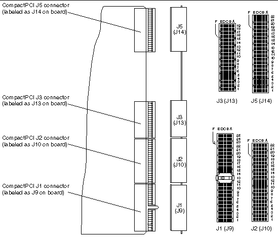
FIGURE B-3 shows contact numbering as seen from the back of the Netra CP2300 board.
FIGURE B-3 Backplane Connector Contact Numbering

|
Note - The CompactPCI J4 connector is not populated on the Netra CP2300 board.
|
B.4.1 CompactPCI J1/P1 (J9) Connector Pinout
The CompactPCI J1 connector is labeled as J9 on the Netra CP2300 board.
TABLE B-10 CompactPCI J1/P1 (J9) Connector Pin Assignments
|
Pin
|
Row Z
|
Row A
|
Row B
|
Row C
|
Row D
|
Row E
|
Row F
|
|
25
|
GND
|
+EP_5V
|
1Volt Prech.
|
VIO Prech.
|
+3.3V
|
+EP_5V
|
GND
|
|
24
|
GND
|
1Volt Prech.
|
+EP_5V
|
LP_VIO
|
1Volt Prech.
|
1Volt Prech.
|
GND
|
|
23
|
GND
|
EP_3.3V
|
1Volt Prech.
|
1Volt Prech.
|
LP_+EP_5V
|
1Volt Prech.
|
GND
|
|
22
|
GND
|
1Volt Prech.
|
GND
|
LP_+EP_3.3V
|
1Volt Prech.
|
1Volt Prech.
|
GND
|
|
21
|
GND
|
+EP_3.3V
|
1Volt Prech.
|
1Volt Prech.
|
1Volt Prech.
|
1Volt Prech.
|
GND
|
|
20
|
GND
|
1Volt Prech.
|
GND
|
VIO
|
1Volt Prech.
|
1Volt Prech.
|
GND
|
|
19
|
GND
|
+EP_3.3V
|
1Volt Prech.
|
1Volt Prech.
|
LP_GND
|
1Volt Prech.
|
GND
|
|
18
|
GND
|
1Volt Prech.
|
GND
|
+EP_3.3V
|
1Volt Prech.
|
1Volt Prech.
|
GND
|
|
17
|
GND
|
+EP_3.3V
|
IPMB SCL
|
IPMB SDA
|
LP_GND
|
1Volt Prech.
|
GND
|
|
16
|
GND
|
1Volt Prech.
|
GND
|
VIO
|
1Volt Prech.
|
1Volt Prech.
|
GND
|
|
15
|
GND
|
+EP_3.3V
|
1Volt Prech.
|
1Volt Prech.
|
BD_SEL_L
|
1Volt Prech.
|
GND
|
|
14
|
Key
|
Key
|
Key
|
Key
|
Key
|
Key
|
Key
|
|
13
|
Key
|
Key
|
Key
|
Key
|
Key
|
Key
|
Key
|
|
12
|
Key
|
Key
|
Key
|
Key
|
Key
|
Key
|
Key
|
|
11
|
GND
|
1Volt Prech.
|
1Volt Prech.
|
1Volt Prech.
|
LP_GND
|
1Volt Prech.
|
GND
|
|
10
|
GND
|
1Volt Prech.
|
GND
|
+EP_3.3V
|
1Volt Prech.
|
1Volt Prech.
|
GND
|
|
9
|
GND
|
1Volt Prech.
|
1Volt Prech.
|
1Volt Prech.
|
LP_GND
|
1Volt Prech.
|
GND
|
|
8
|
GND
|
1Volt Prech.
|
GND
|
VIO
|
1Volt Prech.
|
1Volt Prech.
|
GND
|
|
7
|
GND
|
1Volt Prech.
|
1Volt Prech.
|
1Volt Prech.
|
LP_GND
|
1Volt Prech.
|
GND
|
|
6
|
GND
|
1Volt Prech.
|
PCI_PRES#
|
LP_+EP_3.3V
|
1Volt Prech.
|
1Volt Prech.
|
GND
|
|
5
|
GND
|
BRSVP
|
BRSVP
|
PCI_RST#
|
LP_GND
|
1Volt Prech.
|
GND
|
|
4
|
GND
|
IPMB_PWR
|
HEALTHY
|
LP_VIO
|
intp
|
ints
|
GND
|
|
3
|
GND
|
VIO Prech.
|
VIO Prech.
|
VIO Prech.
|
LP_+EP_5V
|
VIO Prech.
|
GND
|
|
2
|
GND
|
tck
|
+EP_5V
|
tms
|
tdo
|
tdi
|
GND
|
|
1
|
GND
|
+EP_5V
|
-EP_12V
|
trst
|
+EP_12V
|
+EP_5V
|
GND
|
B.4.2 CompactPCI J1/P1 (J9) Signal Descriptions
- 1 Volt Prech: Precharge to 1Volt through individual precharge pull-up resistors, these pins interface to the cPCI bus connector pins.
- VIO Prech: Precharge to EP_3.3V.
- +EP_5V: Backplane power input, EP_5V
- +EP_3.3V: Backplane power input, EP_3.3V
- +EP_12V: Backplane power input, EP_12V
- -EP_12V: Backplane power input, -EP_12V
- VIO: Backplane power input, can be either EP_3.3V or EP_5V
- LP_*: Long pins - see PCIMG Hot Swap Spec R2.0 section 4.2.1
- IPMB_SCL: Independent Platform Management Bus Clock - see CompactPCI System Management Specification PCIMG 2.9 R1.0
- IPMB_SDA: Independent Platform Management Bus Data - see CompactPCI System Management Specification PCIMG 2.9 R1.0
- BD_SEL#: PICMG 2.1 R1.0 Hot-swap signal - pulled up on the board and driven low to enable power on
- IPMB_PWR: Battery back-up power - see CompactPCI System Management Specification PCIMG 2.9 R1.0
- HEALTHY: Radial signal used to acknowledge the health of the board - signals that the board is suitable to be released form reset and allowed onto the bus - see PICMG 2.1 R1.0 Hotswap Spec.
- INTP: Non-cPCI interrupt, legacy IDE - not supported, 1Kohm pull-up provided
- INTS: Non-cPCI interrupt, legacy IDE - not supported
- TCK, TMS, TDO, TDI: JTAG signals, not supported - unconnected.
- BRSVP: Reserve pins - must be left unconnected on backplane
- PCI_PRES#: Used to indicate that the board is plugged into a chassis that supports the cPCI interface.
- PCI_RST#: cPCI interface reset input - in systems that do not support the cPCI interface a 10Kohm pulled is required on the backplane, needs to be pre-charged to VIO.
B.4.3 CompactPCI J2/P2 (J10) Connector Pinout
The CompactPCI J2 connector is labeled as J10 on the Netra CP2300 board.
TABLE B-11 CompactPCI J2/P2 (J10) Connector Pin Assignments
|
Pin
|
Row Z
|
Row A
|
Row B
|
Row C
|
Row D
|
Row E
|
Row F
|
|
22
|
GND
|
GA4
|
GA3
|
GA2
|
GA1
|
GA0
|
GND
|
|
21
|
GND
|
1Volt Prech.
|
GND
|
BRSVP
|
BRSVP
|
1Volt Prech.
|
GND
|
|
20
|
GND
|
1Volt Prech.
|
GND
|
1Volt Prech.
|
GND
|
1Volt Prech.
|
GND
|
|
19
|
GND
|
GND
|
GND
|
SMB_SDA
|
SMB_SCK
|
SMB_ALERT
|
GND
|
|
18
|
GND
|
BRSVP
|
BRSVP
|
1Volt Prech.
|
GND
|
BRSVP
|
GND
|
|
17
|
GND
|
BRSVP
|
GND
|
PRST#
|
1Volt Prech.
|
1Volt Prech.
|
GND
|
|
16
|
GND
|
BRSVP
|
BRSVP
|
DEG#
|
GND
|
BRSVP
|
GND
|
|
15
|
GND
|
BRSVP
|
GND
|
FAL#
|
1Volt Prech.
|
1Volt Prech.
|
GND
|
|
14
|
GND
|
1Volt Prech.
|
1Volt Prech.
|
1Volt Prech.
|
GND
|
1Volt Prech.
|
GND
|
|
13
|
GND
|
1Volt Prech.
|
GND
|
VIO
|
1Volt Prech.
|
1Volt Prech.
|
GND
|
|
12
|
GND
|
1Volt Prech.
|
1Volt Prech.
|
1Volt Prech.
|
GND
|
1Volt Prech.
|
GND
|
|
11
|
GND
|
1Volt Prech.
|
GND
|
VIO
|
1Volt Prech.
|
1Volt Prech.
|
GND
|
|
10
|
GND
|
1Volt Prech.
|
1Volt Prech.
|
1Volt Prech.
|
GND
|
1Volt Prech.
|
GND
|
|
9
|
GND
|
1Volt Prech.
|
GND
|
VIO
|
1Volt Prech.
|
1Volt Prech.
|
GND
|
|
8
|
GND
|
1Volt Prech.
|
1Volt Prech.
|
1Volt Prech.
|
GND
|
1Volt Prech.
|
GND
|
|
7
|
GND
|
1Volt Prech.
|
GND
|
VIO
|
1Volt Prech.
|
1Volt Prech.
|
GND
|
|
6
|
GND
|
1Volt Prech.
|
1Volt Prech.
|
1Volt Prech.
|
GND
|
1Volt Prech.
|
GND
|
|
5
|
GND
|
1Volt Prech.
|
1Volt Prech.
|
VIO
|
1Volt Prech.
|
1Volt Prech.
|
GND
|
|
4
|
GND
|
1Volt Prech.
|
BRSVP
|
1Volt Prech.
|
GND
|
1Volt Prech.
|
GND
|
|
3
|
GND
|
1Volt Prech.
|
GND
|
1Volt Prech.
|
1Volt Prech.
|
1Volt Prech.
|
GND
|
|
2
|
GND
|
1Volt Prech.
|
1Volt Prech.
|
SYSEN#
|
1Volt Prech.
|
1Volt Prech.
|
GND
|
|
1
|
GND
|
1Volt Prech.
|
GND
|
1Volt Prech.
|
1Volt Prech.
|
1Volt Prech.
|
GND
|
B.4.4 CompactPCI J2/P2 (J10) Signal Descriptions
- GA[0..4]: Geographical Addressing signals for unique slot identification
- BRSVP: Reserve pins - leave unconnected on backplane
- SMB_SDA: System Management Data see PICMG 2.9 System Management Bus
- SMB_SCK: System Management Clock see PICMG 2.9 System Management Bus
- SMB_ALERT: cPCI System Management Specification PCIMG 2.9 R1.0 signal.
- PRST#: Backplane Push Button Reset input to the SMC
- DEG#, FAL#: Power Subsystem status signals input to the SMC
- SYSEN#: Used to indicate a slot's capability to support System Host
B.4.5 CompactPCI J3/P3 (J13) Connector Pinout
The CompactPCI J3 connector is labeled as J13 on the Netra CP2300 board.
TABLE B-12 CompactPCI J3/P3 (J13) Connector Pin Assignments
|
Pin
|
Row Z
|
Row A
|
Row B
|
Row C
|
Row D
|
Row E
|
Row F
|
|
19
|
GND
|
RESERVE(GND)
|
RESERVE(GND)
|
RESERVE(GND)
|
RESERVE(GND)
|
GND
|
GND
|
|
18
|
GND
|
PSB_A_TX_POS
|
PSB_A_TX_NEG
|
GND
|
NC
|
NC
|
GND
|
|
17
|
GND
|
PSB_A_RX_POS
|
PSB_A_RX_NEG
|
GND
|
NC
|
NC
|
GND
|
|
16
|
GND
|
PSB_B_TX_POS
|
PSB_B_TX_NEG
|
GND
|
NC
|
NC
|
GND
|
|
15
|
GND
|
PSB_B_RX_POS
|
PSB_B_RX_NEG
|
GND
|
NC
|
NC
|
GND
|
|
14
|
GND
|
+3.3V
|
+3.3V
|
+3.3V
|
+5V
|
+5V
|
GND
|
|
13
|
GND
|
PMC_A_IO<5>
|
PMC_A_IO<4>
|
PMC_A_IO<3>
|
PMC_A_IO<2>
|
PMC_A_IO<1>
|
GND
|
|
12
|
GND
|
PMC_A_IO<10>
|
PMC_A_IO<9>
|
PMC_A_IO<8>
|
PMC_A_IO<7>
|
PMC_A_IO<6>
|
GND
|
|
11
|
GND
|
PMC_A_IO<15>
|
PMC_A_IO<14>
|
PMC_A_IO<13>
|
PMC_A_IO<12>
|
PMC_A_IO<11>
|
GND
|
|
10
|
GND
|
PMC_A_IO<20>
|
PMC_A_IO<19>
|
PMC_A_IO<18.
|
PMC_A_IO<17>
|
PMC_A_IO<16>
|
GND
|
|
9
|
GND
|
PMC_A_IO<25>
|
PMC_A_IO<24>
|
PMC_A_IO<23>
|
PMC_A_IO<22>
|
PMC_A_IO<21>
|
GND
|
|
8
|
GND
|
PMC_A_IO<30>
|
PMC_A_IO<29>
|
PMC_A_IO<28>
|
PMC_A_IO<27>
|
PMC_A_IO<26>
|
GND
|
|
7
|
GND
|
PMC_A_IO<35>
|
PMC_A_IO<34>
|
PMC_A_IO<33>
|
PMC_A_IO<32>
|
PMC_A_IO<31>
|
GND
|
|
6
|
GND
|
PMC_A_IO<40>
|
PMC_A_IO<39>
|
PMC_A_IO<38>
|
PMC_A_IO<37>
|
PMC_A_IO<36>
|
GND
|
|
5
|
GND
|
PMC_A_IO<45>
|
PMC_A_IO<44>
|
PMC_A_IO<43>
|
PMC_A_IO<42>
|
PMC_A_IO<41>
|
GND
|
|
4
|
GND
|
PMC_A_IO<50>
|
PMC_A_IO<49>
|
PMC_A_IO<48>
|
PMC_A_IO<47>
|
PMC_A_IO<46>
|
GND
|
|
3
|
GND
|
PMC_A_IO<55>
|
PMC_A_IO<54>
|
PMC_A_IO<53>
|
PMC_A_IO<52>
|
PMC_A_IO<51>
|
GND
|
|
2
|
GND
|
PMC_A_IO<60>
|
PMC_A_IO<59>
|
PMC_A_IO<58>
|
PMC_A_IO<57>
|
PMC_A_IO<56>
|
GND
|
|
1
|
GND
|
+5V
|
PMC_A_IO<64>
|
PMC_A_IO<63>
|
PMC_A_IO<62>
|
PMC_A_IO<61>
|
GND
|
B.4.6 CompactPCI J3/P3 (J13) Signal Descriptions
- PMC_A[63..0] - PMC/PIM I/O signals
- TPE_A/B_TX/RX_POS/NEG: PCIMG CPSB Node Slot Ethernet Twisted Pair signals (PICMG 2.16 Draft 0.92 CompactPCI Packet Switching Backplane)
- +5V: Backend (SPARC) power VCC
- VDD_3.3V: Backend (SPARC) power 3.3V
- PMC_A_IO<29..1> may also be switched to EIDE port use mutually exclusive with using these pins as PMC_A_IO signals.
B.4.7 CompactPCI J5/P5 (J14) Connector Pinout
The CompactPCI J5 connector is labeled as J14 on the Netra CP2300 board.
TABLE B-13 CompactPCI J5/P5 (J14) Connector Pin Assignments
|
Pin
|
Row Z
|
Row A
|
Row B
|
Row C
|
Row D
|
Row E
|
Row F
|
|
22
|
GND
|
PMC_B_IO<5>
|
PMC_B_IO<4>
|
PMC_B_IO<3>
|
PMC_B_IO<2>
|
PMC_B_IO<1>
|
GND
|
|
21
|
GND
|
PMC_B_IO<10>
|
PMC_B_IO<9>
|
PMC_B_IO<8>
|
PMC_B_IO<7>
|
PMC_B_IO<6>
|
GND
|
|
20
|
GND
|
PMC_B_IO<15>
|
PMC_B_IO<14>
|
PMC_B_IO<13>
|
PMC_B_IO<12>
|
PMC_B_IO<11>
|
GND
|
|
19
|
GND
|
PMC_B_IO<20>
|
PMC_B_IO<19>
|
PMC_B_IO<18>
|
PMC_B_IO<17>
|
PMC_B_IO<16>
|
GND
|
|
18
|
GND
|
PMC_B_IO<25>
|
PMC_B_IO<24>
|
PMC_B_IO<23>
|
PMC_B_IO<22>
|
PMC_B_IO<21>
|
GND
|
|
17
|
GND
|
PMC_B_IO<30>
|
PMC_B_IO<29>
|
PMC_B_IO<28>
|
PMC_B_IO<27>
|
PMC_B_IO<26>
|
GND
|
|
16
|
GND
|
PMC_B_IO<35>
|
PMC_B_IO<34>
|
PMC_B_IO<33>
|
PMC_B_IO<32>
|
PMC_B_IO<31>
|
GND
|
|
15
|
GND
|
PMC_B_IO<40>
|
PMC_B_IO<39>
|
PMC_B_IO<38>
|
PMC_B_IO<37>
|
PMC_B_IO<36>
|
GND
|
|
14
|
GND
|
PMC_B_IO<45>
|
PMC_B_IO<44>
|
PMC_B_IO<43>
|
PMC_B_IO<42>
|
PMC_B_IO<41>
|
GND
|
|
13
|
GND
|
PMC_B_IO<50>
|
PMC_B_IO<49>
|
PMC_B_IO<48>
|
PMC_B_IO<47>
|
PMC_B_IO<46>
|
GND
|
|
12
|
GND
|
PMC_B_IO<55>
|
PMC_B_IO<54>
|
PMC_B_IO<53>
|
PMC_B_IO<52>
|
PMC_B_IO<51>
|
GND
|
|
11
|
GND
|
PMC_B_IO<60>
|
PMC_B_IO<59>
|
PMC_B_IO<58>
|
PMC_B_IO<57>
|
PMC_B_IO<56>
|
GND
|
|
10
|
GND
|
RESERVE
|
PMC_B_IO<64>
|
PMC_B_IO<63>
|
PMC_B_IO<62>
|
PMC_B_IO<61>
|
GND
|
|
9
|
GND
|
SER_A_RTS
|
SER_A_DTR
|
SER_A_RI
|
GND
|
SER_A_CTS
|
GND
|
|
8
|
GND
|
SER_A_DCD
|
SER_A_TXD
|
SER_A_RXD
|
SER_A_DSR
|
+5V
|
GND
|
|
7
|
GND
|
SER_B_RTS
|
SER_B_DTR
|
SER_B_RI
|
SER_B_DSR
|
SER_B_CTS
|
GND
|
|
6
|
GND
|
SER_B_DCD
|
SER_B_TXD
|
SER_B_RXD
|
GND
|
GND
|
GND
|
|
5
|
GND
|
TXN_I2C_CLK
|
RESERVE
|
-12V
|
(NET2_RX_P)
|
(NET2_RX_N)
|
GND
|
|
4
|
GND
|
TXN_I2C_SDA
|
SMC_PWR
|
GND
|
(NET2_TX_P)
|
(NET2_TX_N)
|
GND
|
|
3
|
GND
|
(USB_B_POS)
|
(USB_B_NEG)
|
GND
|
GND
|
GND
|
GND
|
|
2
|
GND
|
USB_A_POS
|
USB_A_NEG
|
GND
|
(NET1_RX_P)
|
(NET1_RX_N)
|
GND
|
|
1
|
GND
|
GND
|
3.3V
|
+12V
|
(NET1_TX_P)
|
(NET1_TX_N)
|
GND
|
B.4.8 CompactPCI J5/P5 (J14) Signal Descriptions
- PMC_B[63..0] - PMC/PIM I/O signals
- +5V: Backend (SPARC) power VCC
- SMC_PWR: Early Power Plane to SMC, 5V for Transition Card I2C Devices
- TXN_I2C_SCL/SDA: I2C data and clock
- VDD_3.3V: Backend (SPARC) power 3.3V
- SER_A/B_RTS: Serial Port TTYA/B Request To Send
- SER_A/B_CTS: Serial Port TTYA/B Clear To Send
- SER_A/B_TX: Serial Port TTYA/B Transmit Data
- SER_A/B_RX: Serial Port TTYA/B Transmit Data
- SER_A/B_DCD: Serial Port TTYA/B Data Carrier Detected
- SER_A/B_DSR: Serial Port TTYA/B Data Set Ready
- SER_A/B_DTR: Serial Port TTYA/B Data Terminal Ready
- SER_A/B_RI: Serial Port TTYA/B Ring Indicator
B.5 DIP Switch Settings
The Netra CP2300 board contains two banks of DIP switches. The SW3 DIP switch is located on the component side of the board and the SW501, SW502, and SW503 DIP switches are located on the solder-side of the board.
B.5.1 SW3 DIP Switch
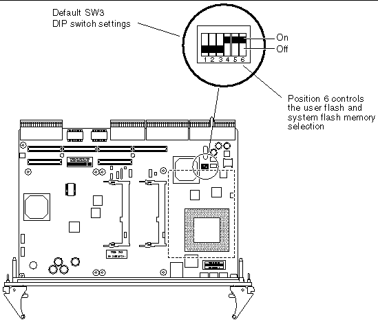
The SW3 DIP switch is a six position switch located on the component side of the Netra CP2300 board. FIGURE B-4 shows the location and default settings of the SW3 DIP switch.
FIGURE B-4 SW3 DIP Switch Location and Default Settings

TABLE B-14 SW3 Position Settings
|
Position #
|
Default Setting
|
Description
|
|
1
|
OFF
|
Proprietary setting. Do not change setting.
|
|
2
|
OFF
|
Proprietary setting. Do not change setting.
|
|
3
|
OFF
|
Proprietary setting. Do not change setting.
|
|
4
|
ON
|
Proprietary setting. Do not change setting.
|
|
5
|
ON
|
Proprietary setting. Do not change setting.
|
|
6
|
ON
|
- ON = Boot the Netra CP2300 board from the standard OpenBoot PROM system flash.
- OFF = Use the SMC firmware programmable variable flash-device to set whether the system flash is selected as bootable in 1 MByte or 7 MBytes of flash memory space.
|
For more information about switching the memory selection between the system flash and the user flash, see Section 4.7.1, Exchanging the System and User Flash Memory Devices.

|
Caution - SW3 DIP switch positions 1 through 5 are not user-selectable and must never be changed. Changing these settings may critically damage the Netra CP2300 board.
|
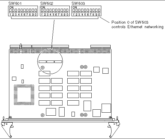
B.5.2 SW501, SW502, and SW503 DIP Switches
The SW501, SW502, and SW503 DIP switches are ten position switches located on the solder side of the Netra CP2300 board. FIGURE B-5 shows the location and default settings of the SW501, SW502, and SW503 DIP switches.
FIGURE B-5 Location and Default Settings of the SW501, SW502, and SW503 DIP Switches

Position 0 of SW503 controls the Ethernet networking on the Netra CP2300 board and transition card. By default, position 0 is set to OFF, which means that the board is set for cPSB network mode and the Netra CP2300 transition card's RJ45 Ethernet ports are disabled. If you will use the Netra CP2300 board in a non-cPSB enclosure, you should set Position 0 of SW503 to ON, so that you can use the RJ45 Ethernet connectors on the transition card.
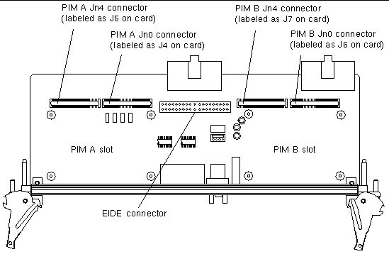
The remaining DIP switch positions (SW501, 1 to 0; SW502, 1 to 0; SW503, 1 to 9) control the EIDE connector on the Netra CP2300 transition card. When these positions are set OFF, you will not be able to use the transition card's EIDE connector. In this setting, however, all of the pin signals (PIM_A_IO_1 to PIM_A_IO_64) on the PIM A Jn4 connector will be available. (The PIM A Jn4 connector is labelled J5 on the transition card.) See FIGURE B-6 for the location of the PIM A Jn4 (J5) and EIDE connectors. Refer to the Netra CP2300 cPSB Transition Card Installation and Technical Reference Manual (816-7188-xx) for the pin descriptions of these connectors.
When these DIP switch positions are set to ON, the EIDE connector on the transition card will be available. However, pins 1 through 29 on the PIM A Jn4 (J5) connector (PIM_A_IO_1 to PIM_A_IO_29) are disabled and must not have PIM A I/O connections.
TABLE B-15 SW501, SW502, SW503 DIP Switch Settings
|
DIP Switch, Position Numbers
|
Default Setting
|
Description
|
|
SW501, positions 1 to 0
SW502, positions 1 to 0
SW503, positions 1 to 9
|
OFF
|
Controls the EIDE and PIM A J5 connectors on the Netra CP2300 transition card.
- OFF = EIDE connector disabled and PIM A J5 connector enabled
- ON = EIDE connector enabled and PIM A Jn4 (J5) connector pins 1 through 29 disabled
|
|
SW503, position 0
|
OFF
|
Controls the RJ45 Ethernet connectors on the Netra CP2300 transition card.
- OFF = cPSB network mode; RJ45 Ethernet connectors disabled
- ON = RJ45 Ethernet connectors enabled
|
|
Note - Even if you are not using the PIM_A_IO connections for transition card PIM applications, the PMC A slot restricts the use of PMC cards with PIM capability. If the PMC card uses the PIM_A_IO_1 to PIM_A_IO_29 signals, refer to your PMC card documentation to determine compatibility.
|
FIGURE B-6 Netra CP2300 cPSB Transition Card EIDE and PIM Connector Locations
