XCP2040-TRN I/O Transition Card Manual for Netra CP2040/CP2140 CompactPCI Boards
|
The XCP2040-TRN I/O Transition Card (806-6743-11) is designed to be used with the Netra CP2040/CP2140 CompactPCI boards and is fully compliant with the CompactPCI Core Specification, Release Note for PICMG 2.0 Revision 3.0 (October 1999, PCI Industrial Computers Manufacturers Group).
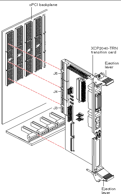
The 6U form factor, single slot transition card supplies rear I/O connection to support additional peripherals with simplified system cabling for use with the compatible CompactPCI system host boards. The rear I/O access also enables the complementary system host boards to be replaced without disconnecting cables. The XCP2040-TRN I/O Transition Card enables the creation of high-density systems by enabling easy access to I/O.
|
Note - It is the responsibility of the system designer to integrate peripheral devices to the connectors on the backplane in a CP2040/CP2140 chassis configuration. A designer can either connect directly to the backplane signals or use a XCP2040-TRN I/O Transition Card.
|
This document contains the following sections:
Features
The XCP2040-TRN I/O Transition Card requires a CompactPCI chassis with a backplane that accommodates front and rear board installation. The primary purpose of this card is to provide the connections to the CP2040/CP2140 board I/O ports. This section lists the important features of the transition card.
These features include:
- Provides access to the I/Os available on cPCI J3, J4, and J5 connectors including two Ethernet ports, two SCSI ports, a parallel port, a floppy header connector, two serial ports, PS2 keyboard/mouse connectors, and two USB ports
|
Note - Some I/O connections are available through the rear panel; others are available through on-board headers.
|
- Meets CompactPCI 6U transition card form factor specifications of 3.1 in. (78.74mm) x 9.2 in. (233.68mm)
- Meets NEBS Level 3 compliance (see the NEBS statement in Installing the Transition Card in a CompactPCI Chassis), FCC Class B, CE, UL, and TUV
- Provides miscellaneous feature headers (I2C, backplane Reset IN/OUT, Tx/Rx) for the System Management Controller (SMC) on the host CP2040/CP2140 board
- Supports I2C EEPROM (64 Kbits) for ID and local environmental monitoring by the SMC for temperature
- Supports A/B cPCI connectors as described in the CompactPCI Core Specification, Release Note for PICMG 2.0 Revision 3.0, "Connectors 2mm Type AB Connector System" section
I/O Interfaces
The XCP2040-TRN I/O Transition Card provides additional I/O features (through the J3, J4, and J5 CompactPCI connector interfaces) to the CP2040/CP2140 board. Many I/O functions are provided on the transition card rear panel, and the rest of the I/O functions are provided from headers mounted on the card.
These functions include:
- One PMC Interface Module (PIM) I/O connector (with user-defined I/O)
- Two 10/100 Fast Ethernet (RJ45) ports available (channel A and channel B)
- Two serial (mini-DB9) ports
- Two Universal Serial Bus ports. Both are accessible directly on the I/O panel.
- One parallel port
- One floppy connector
- Dual SCSI ports
- PS2 keyboard/mouse connector
|
Note - The use of all shielded cables on the transition card is recommended.
|
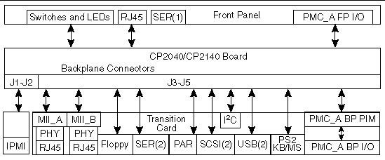
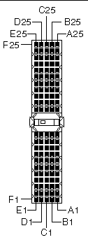
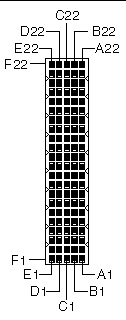
The diagram in Figure 1 shows the I/O interface between the CP2040/CP2140 board, the backplane, and the transition card.
FIGURE 1 Netra CP2040/CP2140 Board I/O Interface
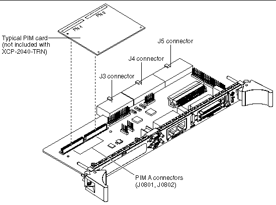
PIM Card Support
FIGURE 2 shows an optional customer-supplied PIM card installed on the
XCP2040-TRN I/O Transition Card.
Features are listed below.
- Supports one single-sized PIM (PMC I/O module) carrier (74mm x 69mm)
- Complies with VITA 36 - PMC I/O Module Standard
See www.vita.com for information on this Web site.
- Allows rear access of PMC I/O
- Leverages IEEE P1386 standard
- Uses 2 x 64 pins connectors (one for PMC I/O, the other power/ground)
- Provides 3.3/5/+ 12/- 12V through the Netra CP2040/CP2140 board
FIGURE 2 Optional PIM Card Placement on XCP2040-TRN I/O Transition Card
SIP Switch Settings
FIGURE 3 shows the default single in-line package (SIP) switch settings on the XCP2040-TRN I/O Transition Card.
FIGURE 3 Default SIP Switch Settings on XCP2040-TRN I/O Transition Card
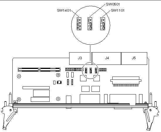
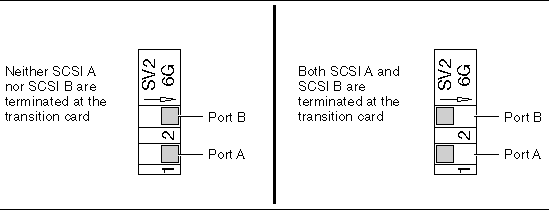
Switch SW1101--SCSI Termination
Switch SW1101 allows the XCP2040-TRN I/O Transition Card to directly terminate the SCSI bus when the CP2040/CP2140 host board is not present in the system. When the CP2040/CP2140 host board is present, the host board provides termination, overriding the transition card switch settings.
When the host board is not present in the system, the transition card can provide termination if the switches are set correctly. TABLE 1 shows the termination settings for the transition card when the host board is not present.
TABLE 1 SCSI Termination Settings for Transition Card
|
Switch Setting
|
Termination
|
|
1 open
|
SCSI A terminated
|
|
1 closed
|
SCSI A not terminated
|
|
2 open
|
SCSI B terminated
|
|
2 closed
|
SCSI B not terminated
|
FIGURE 4 shows possible settings for the SW1101. These switch settings do not affect the termination if the host board is in the system.
FIGURE 4 SW1101 Switch Settings (Example)
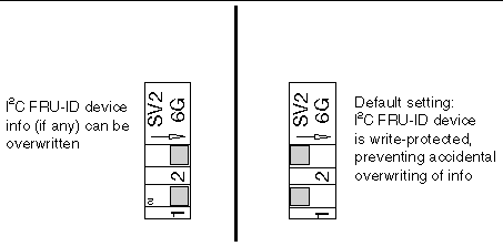
Switch SW1401--I2C Write Protect
Switch SW1401 prevents accidental overwriting of the I2C FRU-ID device once it has been programmed.
FIGURE 5 SW1401 Switch Settings (Example)
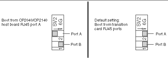
Switch SW0501--Ethernet Boot Selection
The transition card is configured to boot through its own Ethernet port instead of the port on the host CP2040/CP2140 board. You can change this setting with the SW0501 switch. SW0501 selects either the host board RJ45 connector or the transition card RJ45 connector as I/O for Ethernet channel A. There is no RJ45 port B on the host board, so do not move Switch 1, which corresponds to RJ45 port B.
FIGURE 6 SW0501 Switch Settings (Example)

|
Caution - The SW0501 Switch 1 should always be in the closed position.
|
Software Support
The XCP2040-TRN I/O Transition Card is designed to support the CP2040/CP2140 host board. It therefore supports the software supported by the host boards. Please see the Netra CP2040 Technical Reference and Installation Manual (P/N 806-4994-xx) or the Netra CP2140 Technical Reference and Installation Manual (P/N 816-4908-xx) for host board software support.
Specifications
This section provides mechanical, electrical, environmental and other relevant specifications for the XCP2040-TRN I/O Transition Card.
Mechanical Dimensions
TABLE 2 provides physical dimensions for the XCP2040-TRN I/O Transition Card.
TABLE 2 Physical Dimensions
|
Board Specifications
|
Dimensions
|
|
Form Factor
|
6U
|
|
Length
|
9.2 inches (233.68 mm)
|
|
Width
|
3.1 inches (78.74 mm)
|
|
Height
|
0.54 inches (13.716 mm)
|
Power Requirements
The XCP2040-TRN I/O Transition Card is powered through the CP2040/CP2140 board, which provides the following voltage: 5V/3.3V/12V/-12V (maximum 2.5 W). For more information, see the Netra CP2040 Technical Reference and Installation Manual (P/N 806-4994-xx) or the Netra CP2140 Technical Reference and Installation Manual (P/N 816-4908-xx).
The XCP2040-TRN I/O Transition Card has mainly passive components. However, some power from the backplane is provided to the PIM carrier, the I2C EEPROM, the PHY ICs, and the SCSI terminators.
For information on PIM allowable dissipation and limits on PIM power consumption, see VITA 36, PMC I/O Module Standard.
Environmental Specifications, Compliance, Reliability, and Availability
For details on the environmental specifications, compliance, reliability, and availability, please see the Specifications chapter of the Netra CP2040 Technical Reference and Installation Manual (P/N 806-4994-xx) or the Netra CP2140 Technical Reference and Installation Manual (P/N 816-4908-xx).
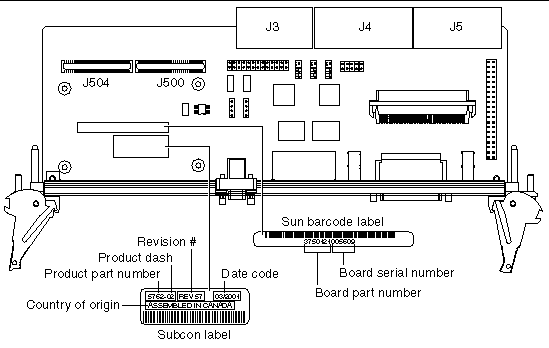
Determining Part Number, Serial Number, and Revision Number
The XCP2040-TRN I/O Transition Card part number, serial number, and revision can be found on stickers located on the card labels. For proper identification of the card, please see the list below and FIGURE 7. The barcode labels provide the following information:
The Sun Microsystems barcode label provides the following information:
- Card part number (for example, 3750120), which is the first seven digits on the barcode label
- Card serial number (for example, 005609), which is the next six digits on the barcode label
The Subcon barcode label provides the following information:
- Product part number (for example, 5762), product dash (for example, 02) and revision number (for example REV 57)
- Card date code (for example, 03/2001), which represents the third week of year 2001
- Country of origin (for example, ASSEMBLED IN CANADA)
FIGURE 7 Identification Labels on the XCP2040-TRN I/O Transition Card
Connectors
This section provides connector pinouts for both the external rear-panel connectors and on-board connectors for the XCP2040-TRN I/O Transition Card.
Upgrading Backplanes for PICMG Compliance
The system that you are installing the XCP2040-TRN I/O Transition Card into must have connectors that meet the PICMG 2.0 Revision 3.0 specification. You can upgrade the backplane connectors by using a shroud removal tool, such as provided by the Erni Companies. For additional information on the Erni company products, visit the following Web page:
http://connect.erni.com/
Transition Card I/O Rear Panel Connectors
This section lists the pins and signal names of the I/O rear panel connectors on the transition card.
FIGURE 8 XCP2040-TRN I/O Transition Card Rear Panel Connectors
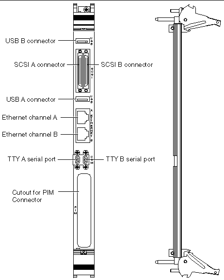
USB Ports
TABLE 3 and TABLE 4 provide signal descriptions for USB connectors, Port A and Port B.
TABLE 3 Universal Serial Bus Port A (J1003) Signal Descriptions
|
Pin
|
Signal
|
|
1
|
USB1VDD (PWR)
|
|
2
|
USB1D-(N_CON)
|
|
3
|
USB1D+ (P_CON)
|
|
4
|
USB1_GND
|
TABLE 4 Universal Serial Bus Port B (J1005) Signal Descriptions
|
Pin
|
Signal
|
|
1
|
USB2VDD (PWR)
|
|
2
|
USB2D-(N_CON)
|
|
3
|
USB2D+ (P_CON)
|
|
4
|
USB2_GND
|
Serial Ports
Two serial ports from the CP2040/CP2140 board Super I/O PC97307 are available through the rear panel with two stacked mini 9-pin connectors. One connector is assigned to Port A and the other connector to Port B. The signal interface of the connector is as follows:
TABLE 5 Dual 16550 Compatible UARTs for Serial Ports (J1006) Signal Descriptions
|
Serial A of Dual Connector
|
|
Serial B of Dual Connector
|
|
Pin
|
Signal
|
|
Pin
|
Signal
|
|
P1A
|
DCDA
|
|
P1B
|
DCDB
|
|
P2A
|
RXDA
|
|
P2B
|
RXDB
|
|
P3A
|
TXDA
|
|
P3B
|
TXDB
|
|
P4A
|
DTRA
|
|
P4B
|
DTRB
|
|
P5A
|
DGNDA
|
|
P5B
|
DGNDB
|
|
P6A
|
DSRA
|
|
P6B
|
DSRB
|
|
P7A
|
RTSA
|
|
P7B
|
RTSB
|
|
P8A
|
CTSA
|
|
P8B
|
CTSB
|
|
P9A
|
RIA
|
|
P9B
|
RIB
|
|
Note - The two serial ports require the use of specific adapter cables. Use the Serial Cable Adapter, MDSM-9F to DB9M, (6 inch 9 wires), P/N C-CEL-10110-10. The manufacturer is Computer Cable Makers Inc. and can be ordered directly through them.
|
Fast Ethernet
The dual jack RJ45 Ethernet (J701) AMP1116353-8 pin locations are shown FIGURE 9 and the signal descriptions are listed in TABLE 6.
FIGURE 9 RJ45 Standard Ethernet Connector
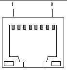
TABLE 6 Fast Ethernet Ports A and B Signal Descriptions
|
Ethernet Port A
|
|
Ethernet Port B
|
|
Pin
|
Signal
|
|
Pin
|
Signal
|
|
1
|
TP_B_T_POS_C
|
|
1
|
TP_A_TX_POS_C
|
|
2
|
TP_B_T_NEG_C
|
|
2
|
TP_A_TX_NEG_C
|
|
3
|
TP_B_R_POS_C
|
|
3
|
TP_A_RX_POS_C
|
|
4
|
CH_GND
|
|
4
|
CH_GND
|
|
5
|
CH_GND
|
|
5
|
CH_GND
|
|
6
|
TP_B_R_NEG_C
|
|
6
|
TP_A_RX_NEG_C
|
|
7
|
CH_GND
|
|
7
|
CH_GND
|
|
8
|
CH_GND
|
|
8
|
CH_GND
|
SCSI Connectors
Two 68-pin Ultra Wide SCSI connectors (A and B) are provided on the rear panel for external device interface through an external, mini dual SCSI connector at J0901. The SCSI connectors have a direct wire from CP2040/CP2140 backplane signal.
FIGURE 10 shows the SCSI connector pin locations and TABLE 7 shows the signal descriptions for the SCSI connector pins.
FIGURE 10 External Ultra Wide SCSI Connector
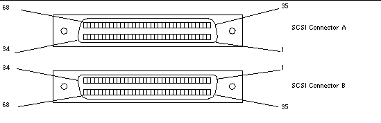
TABLE 7 Rear Panel and Internal Ultra Wide SCSI Connector (J2001) Signal Descriptions
|
Pin #
|
Signal Name
|
|
Pin #
|
Signal Name
|
|
Pin #
|
Signal Name
|
|
1
|
DGND
|
|
24
|
DGND
|
|
47
|
DB7
|
|
2
|
DGND
|
|
25
|
DGND
|
|
48
|
DBP
|
|
3
|
DGND
|
|
26
|
DGND
|
|
49
|
DGND
|
|
4
|
DGND
|
|
27
|
DGND
|
|
50
|
DGND
|
|
5
|
DGND
|
|
28
|
DGND
|
|
51
|
TermP
|
|
6
|
DGND
|
|
29
|
DGND
|
|
52
|
TermP
|
|
7
|
DGND
|
|
30
|
DGND
|
|
53
|
N/C
|
|
8
|
DGND
|
|
31
|
DGND
|
|
54
|
DGND
|
|
9
|
DGND
|
|
32
|
DGND
|
|
55
|
ATN
|
|
10
|
DGND
|
|
33
|
DGND
|
|
56
|
DGND
|
|
11
|
DGND
|
|
34
|
DGND
|
|
57
|
BSY
|
|
12
|
DGND
|
|
35
|
DB12
|
|
58
|
ACK
|
|
13
|
DGND
|
|
36
|
DB13
|
|
59
|
RST
|
|
14
|
DGND
|
|
37
|
DB14
|
|
60
|
MSG
|
|
15
|
DGND
|
|
38
|
DB15
|
|
61
|
SEL
|
|
16
|
DGND
|
|
39
|
DBP1
|
|
62
|
C/D
|
|
17
|
TermP
|
|
40
|
DB0
|
|
63
|
REQ
|
|
18
|
TermP
|
|
41
|
DB1
|
|
64
|
I/O
|
|
19
|
N/C
|
|
42
|
DB2
|
|
65
|
DB8
|
|
20
|
DGND
|
|
43
|
DB3
|
|
66
|
DB9
|
|
21
|
DGND
|
|
44
|
DB4
|
|
67
|
DB10
|
|
22
|
DGND
|
|
45
|
DB5
|
|
68
|
DB11
|
|
23
|
DGND
|
|
46
|
DB6
|
|
|
|
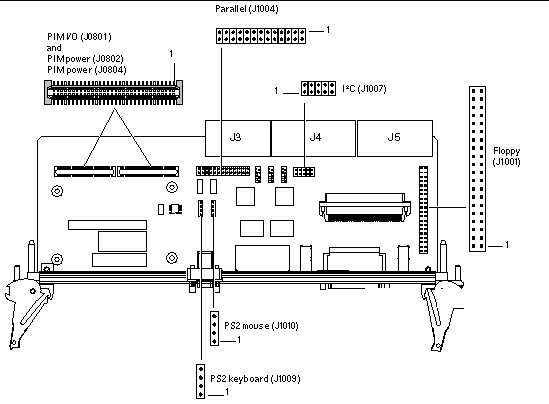
On-Board Interfaces/Connectors on
XCP2040-TRN I/O Transition Card
FIGURE 11 shows the on-board connectors for the XCP2040-TRN I/O Transition Card.
FIGURE 11 XCP2040-TRN I/O Transition Card On-Board Connectors and Interfaces
I2C Bus Access Header
The I2C bus access header pin locations are shown in . The signal descriptions are listed in TABLE 8.
FIGURE 12 I2C Bus Access Header Pin Locations
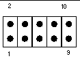
TABLE 8 I2C Bus Access Header (J1007) Signal Descriptions
|
Pin
|
Signal
|
|
1
|
I2C_BP_J4_SDA
|
|
2
|
GND
|
|
3
|
I2C_BP_J4_SCL
|
|
4
|
XIR_L
|
|
5
|
I2C_PWR
|
|
6
|
DIAG_L_OC
|
|
7
|
I2C_PWR
|
|
8
|
BP_BKRST_OUT_L
|
|
9
|
GND
|
|
10
|
BP_BKRST_IN_L
|
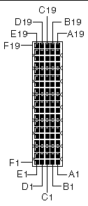
PIM Connectors
The PIM has two 64 pin connectors at J0800 and J0804. The pin locations for both connectors are shown in FIGURE 13. The signal descriptions are listed in TABLE 9 and TABLE 10.
FIGURE 13 PIM Connector Pin Locations
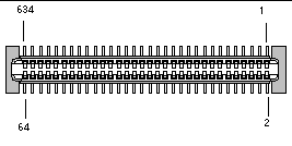
TABLE 9 PIM Connector (J4/J0804) Signal Descriptions
|
Pin
|
Signal
|
|
Pin
|
Signal
|
|
Pin
|
Signal
|
|
1
|
PMC_A_IO1
|
|
23
|
PMC_A_IO23
|
|
45
|
PMC_A_IO45
|
|
2
|
PMC_A_IO2
|
|
24
|
PMC_A_IO24
|
|
46
|
PMC_A_IO46
|
|
3
|
PMC_A_IO3
|
|
25
|
PMC_A_IO25
|
|
47
|
PMC_A_IO47
|
|
4
|
PMC_A_IO4
|
|
26
|
PMC_A_IO26
|
|
48
|
PMC_A_IO48
|
|
5
|
PMC_A_IO5
|
|
27
|
PMC_A_IO27
|
|
49
|
PMC_A_IO49
|
|
6
|
PMC_A_IO6
|
|
28
|
PMC_A_IO28
|
|
50
|
PMC_A_IO50
|
|
7
|
PMC_A_IO7
|
|
29
|
PMC_A_IO29
|
|
51
|
PMC_A_IO51
|
|
8
|
PMC_A_IO8
|
|
30
|
PMC_A_IO30
|
|
52
|
PMC_A_IO52
|
|
9
|
PMC_A_IO9
|
|
31
|
PMC_A_IO31
|
|
53
|
PMC_A_IO53
|
|
10
|
PMC_A_IO10
|
|
32
|
PMC_A_IO32
|
|
54
|
PMC_A_IO54
|
|
11
|
PMC_A_IO11
|
|
33
|
PMC_A_IO33
|
|
55
|
PMC_A_IO55
|
|
12
|
PMC_A_IO12
|
|
34
|
PMC_A_IO34
|
|
56
|
PMC_A_IO56
|
|
13
|
PMC_A_IO13
|
|
35
|
PMC_A_IO35
|
|
57
|
PMC_A_IO57
|
|
14
|
PMC_A_IO14
|
|
36
|
PMC_A_IO36
|
|
58
|
PMC_A_IO58
|
|
15
|
PMC_A_IO15
|
|
37
|
PMC_A_IO37
|
|
59
|
PMC_A_IO59
|
|
16
|
PMC_A_IO16
|
|
38
|
PMC_A_IO38
|
|
60
|
PMC_A_IO60
|
|
17
|
PMC_A_IO17
|
|
39
|
PMC_A_IO39
|
|
61
|
PMC_A_IO61
|
|
18
|
PMC_A_IO18
|
|
40
|
PMC_A_IO40
|
|
62
|
PMC_A_IO62
|
|
19
|
PMC_A_IO19
|
|
41
|
PMC_A_IO41
|
|
63
|
PMC_A_IO63
|
|
20
|
PMC_A_IO20
|
|
42
|
PMC_A_IO42
|
|
64
|
PMC_A_IO64
|
|
21
|
PMC_A_IO21
|
|
43
|
PMC_A_IO43
|
|
|
|
|
22
|
PMC_A_IO22
|
|
44
|
PMC_A_IO44
|
|
|
|
TABLE 10 PIM Connector (J0/J0800) Signal Descriptions
|
Pin
|
Signal
|
|
Pin
|
Signal
|
|
Pin
|
Signal
|
|
1
|
BP_SMC_TX
|
|
23
|
NC
|
|
45
|
SIG_GND
|
|
2
|
BP_12V_POS
|
|
24
|
NC
|
|
46
|
NC
|
|
3
|
BP_SMC_RX
|
|
25
|
NC
|
|
47
|
NC
|
|
4
|
NC
|
|
26
|
BP_3.3V
|
|
48
|
NC
|
|
5
|
BP_5V
|
|
27
|
NC
|
|
49
|
NC
|
|
6
|
NC
|
|
28
|
NC
|
|
50
|
SIG_GND
|
|
7
|
I2C_BP_JS_SDA
|
|
29
|
SIG_GND
|
|
51
|
NC
|
|
8
|
NC
|
|
30
|
NC
|
|
52
|
NC
|
|
9
|
I2C_BP_JS_SCL
|
|
31
|
NC
|
|
53
|
BP_5V
|
|
10
|
BP_3.3V
|
|
32
|
NC
|
|
54
|
NC
|
|
11
|
I2C_PWR
|
|
33
|
NC
|
|
55
|
NC
|
|
12
|
NC
|
|
34
|
SIG_GND
|
|
56
|
NC
|
|
13
|
SIG_GND
|
|
35
|
NC
|
|
57
|
NC
|
|
14
|
NC
|
|
36
|
NC
|
|
58
|
BP_3.3V
|
|
15
|
USB_NEG
|
|
37
|
BP_5V
|
|
59
|
NC
|
|
16
|
NC
|
|
38
|
NC
|
|
60
|
NC
|
|
17
|
USB_POS
|
|
39
|
NC
|
|
61
|
BP_12V_NEG
|
|
18
|
SIG_GND
|
|
40
|
NC
|
|
62
|
NC
|
|
19
|
NC
|
|
41
|
NC
|
|
63
|
NC
|
|
20
|
NC
|
|
42
|
BP_3.3V
|
|
64
|
NC
|
|
21
|
BP_5V
|
|
43
|
NC
|
|
|
|
|
22
|
NC
|
|
44
|
NC
|
|
|
|
On-board SCSI Connector
An on-board 1 x 68-pin Ultra Wide internal right-angled (SCSI A) connector at J0902 is provided for internal devices. This is an electrically redundant connector to the SCSI A port on the rear panel. Only one of these SCSI A connectors should be used at a time to avoid long unterminated stubs on the SCSI chain.
See FIGURE 10 for SCSI connector pin locations and TABLE 7 for signal descriptions for the internal SCSI connector.
Parallel Port
An internal parallel port connection is available through the XCP2040-TRN I/O Transition Card through an on-board header at J1004. The parallel interface is not brought to the rear panel on a single-slot rear panel. shows the internal parallel port header connector.
The parallel port has the following features:
- Direct wire from CP2040/CP2140 backplane signal
- IEEE 1284-compatible interface standard
|
Note - The IEEE1284-compatible printer interconnect cable should not exceed 9 feet.
|
The pin locations for the parallel port are shown in and the signal descriptions are listed in TABLE 11.
FIGURE 14 Internal Parallel Port Header Connector (J1004) Pin Locations
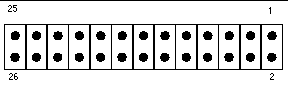
TABLE 11 Parallel Port Signal Descriptions
|
Pin #
|
Signal Name
|
|
Pin #
|
Signal Name
|
|
1
|
PAR_STB_F
|
|
2
|
PAR_AFD_F
|
|
3
|
PAR_D0_F
|
|
4
|
PAR_ERR_F
|
|
5
|
PAR_D1_F
|
|
6
|
PAR_INIT_F
|
|
7
|
PAR_D2_F
|
|
8
|
PAR_SLIN_F
|
|
9
|
PAR_D3_F
|
|
10
|
GND
|
|
11
|
PAR_D4_F
|
|
12
|
GND
|
|
13
|
PAR_D5_F
|
|
14
|
GND
|
|
15
|
PAR_D6_F
|
|
16
|
GND
|
|
17
|
PAR_D7_F
|
|
18
|
GND
|
|
19
|
PAR_ACK_F
|
|
20
|
GND
|
|
21
|
PAR_BUSY_F
|
|
22
|
GND
|
|
23
|
PAR_PE_F
|
|
24
|
GND
|
|
25
|
PAR_SLCT_F
|
|
26
|
GND
|
Floppy Header Connector
The pin locations for the floppy header connector are shown in FIGURE 15 and the signal descriptions are listed in TABLE 12.
FIGURE 15 Floppy Connector Pin Locations
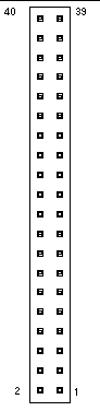
TABLE 12 Floppy Connector Signal Descriptions
|
Pin #
|
Signal Name
|
|
Pin #
|
Signal Name
|
|
1
|
DGND
|
|
2
|
DENSEL
|
|
3
|
DGND
|
|
4
|
N/C
|
|
5
|
DGND
|
|
6
|
DRATE0_MSEN0
|
|
7
|
DGND
|
|
8
|
INDEX
|
|
9
|
DGND
|
|
10
|
DS0
|
|
11
|
DGND
|
|
12
|
DS1
|
|
13
|
DGND
|
|
14
|
DS0
|
|
15
|
DGND
|
|
16
|
MTR0
|
|
17
|
DRATE1_MSEN1
|
|
18
|
DIR
|
|
19
|
DGND
|
|
20
|
STEP
|
|
21
|
DGND
|
|
22
|
WDATA
|
|
23
|
DGND
|
|
24
|
WGATE
|
|
25
|
DGND
|
|
26
|
TR0
|
|
27
|
DRATE0_MSEN0
|
|
28
|
WPROT
|
|
29
|
DGND
|
|
30
|
RDATA
|
|
31
|
DGND
|
|
32
|
HDSEL
|
|
33
|
DGND
|
|
34
|
DSKCHG
|
|
35
|
DGND
|
|
36
|
DGND
|
|
37
|
DGND
|
|
38
|
VCC
|
|
39
|
DGND
|
|
40
|
VCC
|
Backplane Interface
The XCP2040-TRN I/O transition card interfaces to the CompactPCI bus through J3, J4, and J5 connectors. The pin assignments for these three sets of connectors are provided in this section.
J3 Connector
The pin locations for the J3 connector are shown in FIGURE 16.
FIGURE 16 J3 Connector Pin Location
The signal descriptions for the J3 connector are shown in TABLE 13.
TABLE 13 J3/P3 Connector Signal Descriptions
|
Pin #
|
Row Z
|
Row A
|
Row B
|
Row C
|
Row D
|
Row E
|
Row F
|
|
19
|
GND
|
PMC-1
|
PMC-2
|
PMC-3
|
PMC-4
|
PMC-5
|
GND
|
|
18
|
GND
|
PMC-6
|
PMC-7
|
PMC-8
|
PMC-9
|
PMC-10
|
GND
|
|
17
|
GND
|
PMC-11
|
PMC-12
|
PMC-13
|
PMC-14
|
PMC-15
|
GND
|
|
16
|
GND
|
PMC-16
|
PMC-17
|
PMC-18
|
PMC-19
|
PMC-20
|
GND
|
|
15
|
GND
|
PMC-21
|
PMC-22
|
PMC-23
|
PMC-24
|
PMC-25
|
GND
|
|
14
|
GND
|
PMC-26
|
PMC-27
|
PMC-28
|
PMC-29
|
PMC-30
|
GND
|
|
13
|
GND
|
PMC-31
|
PMC-32
|
PMC-33
|
PMC-34
|
PMC-35
|
GND
|
|
12
|
GND
|
PMC-36
|
PMC-37
|
PMC-38
|
PMC-39
|
PMC-40
|
GND
|
|
11
|
GND
|
PMC-41
|
PMC-42
|
PMC-43
|
PMC-44
|
PMC-45
|
GND
|
|
10
|
GND
|
PMC-46
|
PMC-47
|
PMC-48
|
PMC-49
|
PMC-50
|
GND
|
|
9
|
GND
|
PMC-51
|
PMC-52
|
PMC-53
|
PMC-54
|
PMC-55
|
GND
|
|
8
|
GND
|
PMC-56
|
PMC-57
|
PMC-58
|
PMC-59
|
PMC-60
|
GND
|
|
7
|
GND
|
PMC-61
|
PMC-62
|
PMC-63
|
PMC-64
|
VI/O
|
GND
|
|
6
|
GND
|
BD_SEL_5#
|
HEALTHY_5#
|
PCI_RST_5#
|
|
|
GND
|
|
5
|
GND
|
BD_SEL_4#
|
HEALTHY_4#
|
PCI_RST_4#
|
|
|
GND
|
|
4
|
GND
|
BD_SEL_3#
|
HEALTHY_3#
|
PCI_RST_3#
|
|
|
GND
|
|
3
|
GND
|
BD_SEL_2#
|
HEALTHY_2#
|
PCI_RST_2#
|
PCIB_RST_L
|
PCI_RST_6#
|
GND
|
|
2
|
GND
|
BD_SEL_1#
|
HEALTHY_1#
|
PCI_RST_1#
|
EP_5V
|
HEALTHY_6#
|
GND
|
|
1
|
GND
|
BD_SEL_0#
|
HEALTHY_0#
|
PCI_RST_0#
|
|
BD_SEL_6#
|
GND
|
J4 Connector
The pin assignments for the J4 connector are shown in FIGURE 17.
FIGURE 17 J4 Connector Pin Locations
The signal descriptions for the J4 connector are shown in TABLE 14.
TABLE 14 J4/P4 Connector Signal Descriptions
|
Pin #
|
Row Z
|
Row A
|
Row B
|
Row C
|
Row D
|
Row E
|
Row F
|
|
25
|
GND
|
MIIA_CRS
|
MIIA_COL
|
MIIA_MDIO_L
|
MIIA_TX_ERS
|
+5V
|
GND
|
|
24
|
GND
|
MIIA_RX_DV
|
MIIA_RX_ER
|
MIIA_TX_CLKI
|
GND
|
BP_MCA_INT_L
|
GND
|
|
23
|
GND
|
MIIA_RXD1
|
MIIA_RXD2
|
GND
|
MIIA_RXD3
|
MIIA_RX_CLK
|
GND
|
|
22
|
GND
|
GND
|
MIIA_TXD0
|
MIIA_TX_EN
|
MIIA_MDC
|
MIIA_RXD0
|
GND
|
|
21
|
GND
|
MIIA_TXD3
|
GND
|
MIIA_TXD2
|
GND
|
MIIA_TXD1
|
GND
|
|
20
|
GND
|
|
|
I2C_INT_L
|
GND
|
FR/BK_SEL
|
GND
|
|
19
|
GND
|
MIIB_COL
|
MIIB_MDIO_L
|
MIIB_TX_ER
|
|
|
GND
|
|
18
|
GND
|
MIIB_RX_CLK
|
MIIB_RX_DV
|
MIIB_RX_ER
|
MIIB_TX_CLKI
|
MIIB_CRS
|
GND
|
|
17
|
GND
|
MIIB_RXD0
|
GND
|
MIIB_RXD1
|
MIIB_RXD2
|
MIIB_RXD3
|
GND
|
|
16
|
GND
|
MIIB_TXD1
|
MIIB_TXD0
|
MIIB_TX_EN
|
MIIB_MDC
|
GND
|
GND
|
|
15
|
GND
|
GND
|
+5V
|
+5V
|
MIIB_TXD3
|
MIIB_TXD2
|
GND
|
|
14
|
KEY
|
|
|
|
|
|
KEY
|
|
13
|
KEY
|
|
|
|
|
|
KEY
|
|
12
|
KEY
|
|
|
|
|
|
KEY
|
|
11
|
GND
|
BP_TYPE0
|
BP_TYPE1
|
I2C_SDA
|
GND
|
GND
|
GND
|
|
10
|
GND
|
SMC_TX
|
SMC_RX
|
BP_PWROFF
|
I2C_PWR
|
+12V
|
GND
|
|
9
|
GND
|
GND
|
GND
|
I2C_SCL
|
TRM_PWR
|
TRM2_PWR
|
GND
|
|
8
|
GND
|
SCDPH_L
|
SCD<15>_L
|
SCD<14>_L
|
SCD<13>_L
|
SCD<12>_L
|
GND
|
|
7
|
GND
|
SCD<4>_L
|
SCD<3>_L
|
SCD<2>_L
|
SCD<1>_L
|
SCD<0>_L
|
GND
|
|
6
|
GND
|
GND
|
SCDPL_L
|
SCD<7>_L
|
SCD<6>_L
|
SCD<5>_L
|
GND
|
|
5
|
GND
|
GND
|
RSV_MCU-use
|
+5V
|
+5V
|
RSV_MCU-use
|
GND
|
|
4
|
GND
|
SRST_L
|
ACK_L
|
BSY_L
|
GND
|
ATN_L
|
GND
|
|
3
|
GND
|
I/O_L
|
REQ_L
|
C/D_L
|
SEL_L
|
MSG_L
|
GND
|
|
2
|
GND
|
RESERVED
|
SCD<11>_L
|
SCD<10>_L
|
SCD<9>_L
|
SCD<8>_L
|
GND
|
|
1
|
GND
|
RSV-MCU-use
|
RSV-MCU-use
|
+3.3V
|
-12V
|
GPIOI-RSV-MCU-use
|
GND
|
J5 Connector
The pin locations for the J5 connector are shown in FIGURE 18.
FIGURE 18 J5 Connector Pin Locations
The signal descriptions for the J5 connector and are listed in TABLE 15.
TABLE 15 J5/P5 Connector Signal Descriptions
|
Pin #
|
Row Z
|
Row A
|
Row B
|
Row C
|
Row D
|
Row E
|
Row F
|
|
22
|
GND
|
BKRST_IN_L
|
GND
|
DIAG_L_OC
|
+5V
|
BP_XIR_L
|
GND
|
|
21
|
GND
|
KBDDAT
|
KBDCLK
|
KBDVCC
|
AUXDATA
|
AUXCLK
|
GND
|
|
20
|
GND
|
+5V
|
UBS1_P
|
USB1_N
|
KBDGND
|
INT_2#
|
GND
|
|
19
|
GND
|
PAR_DS_L
|
GND
|
+5V
|
INT_0#
|
INT_1#
|
GND
|
|
18
|
GND
|
AFD_L
|
USB2_P
|
USB2_N
|
GND
|
+5V
|
GND
|
|
17
|
GND
|
PD<2>
|
INIT_L
|
PD<1>
|
ERR
|
PD<0>
|
GND
|
|
16
|
GND
|
PD<6>
|
PD<5>
|
PD<4>
|
PD<3>
|
SLIN_L
|
GND
|
|
15
|
GND
|
SLCT
|
PE
|
BUSY_L
|
ACK_L
|
PD<7>
|
GND
|
|
14
|
GND
|
RTSA
|
CTSA
|
RIA
|
GND
|
DTRA
|
GND
|
|
13
|
GND
|
DCDA
|
+5V
|
RXDA
|
DSRA
|
TXDA
|
GND
|
|
12
|
GND
|
RTSB
|
CTSB
|
RIB
|
+5V
|
DTRB
|
GND
|
|
11
|
GND
|
DCDB
|
GND
|
RXDB
|
DSRB
|
TXDB
|
GND
|
|
10
|
GND
|
TR0_L
|
WPROT_L
|
RDATA_L
|
HDSEL_L
|
DSKCHG_L
|
GND
|
|
9
|
GND
|
MTR1_L
|
DIR_L
|
STEP_L
|
WDATA_L
|
WGATE_L
|
GND
|
|
8
|
GND
|
DRVDENS1
|
INDEX_L
|
MTR0_L
|
DS1_L
|
DRV0_SEL_L
|
GND
|
|
7
|
GND
|
DRATE0
|
SC2D<2>_L
|
SC2D<1>_L
|
SC2D<0>_L
|
DENSELO
|
GND
|
|
6
|
GND
|
SC2D<6>_L
|
GND
|
SC2D<5>_L
|
SC2D<4>_L
|
SC2D<3>_L
|
GND
|
|
5
|
GND
|
SC2D<10>_L
|
SC2D<9>_L
|
SC2D<8>_L
|
SC2DPL_L
|
SC2D<7>_L
|
GND
|
|
4
|
GND
|
SC2D<13>_L
|
SC2D<12>_L
|
GND
|
MSEN0
|
SC2D<11>_L
|
GND
|
|
3
|
GND
|
Term2_Disable
|
SC2DPH_L
|
SC2D<15>_L
|
MSEN1
|
SC2D<14>_L
|
GND
|
|
2
|
GND
|
I/O2_L
|
REQ2_L
|
C/D2_L
|
SEL2_L
|
MSG2_L
|
GND
|
|
1
|
GND
|
BKRST_OUT_L
|
SRST2_L
|
ACK2_L
|
BUSY2_L
|
ATN2_L
|
GND
|
TABLE 16 and TABLE 17 list some of the signal definitions for the J4 and J5 connectors.
TABLE 16 Signal Definitions
|
Signal Abbreviation
|
Signal Description
|
|
MII_RXD<0:3>
|
Receive data
|
|
MII_TXD<0:3>
|
Transmit data
|
|
MII_RX_CLK
|
Receive clock
|
|
MII_TX_CLKI
|
Transmit clock
|
|
MII_TX_EN
|
Transmit enable
|
|
MII_CRS
|
Carrier sense
|
|
MII_COL
|
Collision detect
|
|
MII_RX_ER
|
Receive error
|
|
MII_TX_ER
|
Transmit error
|
|
MII_RX_DV
|
Receive frame detect
|
|
MII_MDIO
|
Transceiver management data (external)
|
TABLE 17 SCSI, X3T10 SPI/Single-ended Levels
|
Signal Abbreviation
|
Signal Description
|
|
ATN
|
Attention - Active low
|
|
BSY
|
Busy - Active low
|
|
C/D
|
Command or Data - Active low
|
|
I/O
|
Input or output data direction
|
|
MSG
|
Message phase indicator - Active low
|
|
ACK
|
Acknowledge - Active low
|
|
SCD<0:15>
|
SCSI data lines - Active low
|
|
SCDPH
|
SCSI parity high byte; provides parity for SCD[8:15] - Active low
|
|
SCDPL
|
SCSI parity low byte; provides parity for SCD[0:7] - Active low
|
|
SEL
|
Select - Active low
|
|
REQ
|
Request - Active low
|
|
SRST
|
SCSI bus reset - Active low
|
|
TRM_PWR
|
Termination power for external SCSI terminator
|
PIM Card Interface
The XCP2040-TRN I/O transition card supports a PMC I/O module (PIM). A PIM is generally located on a transition card to enable rear I/O from the CompactPCI bus chassis. Custom PIMs provide additional I/Os that do not fit on the standard transition card rear panel. (For more information on PIM slot mechanics, electrical and logical information, see VITA 36 - PMC I/O Module Standard available http://www.vita.com and the IEEE P1386 Standard). The single-sized PIM measures 2.92 inches (74 mm) wide and 2.72 inches (69 mm) deep.
The J3 I/O on the host board, through the PIM card on the transition card, provides matching I/O on the enclosure backpanel. The signals are routed through the CompactPCI J3 connector.
The PIM card must be mounted on the transition card before the XCP2040-TRN is inserted in a CompactPCI system.

|
Caution - A PIM card must be used with its matching PMC. Any other combination could lead to damage of the PIM or PMC.
|
FIGURE 19 Typical PIM Card and Connectors on XCP2040-TRN I/O Transition Card

|
Note - The PIM cards shown in FIGURE 2 and FIGURE 19 are examples only and are not included with the XCP2040-TRN I/O transition card shipment.
|
Installing the Transition Card in a CompactPCI Chassis
Please keep the following in mind before installing the XCP2040-TRN I/O Transition Card into a system chassis:
- The XCP2040-TRN I/O Transition Card installs into a CompactPCI chassis with a backplane made for front and rear board installation. The CompactPCI backplane must be PICMG 2.0 Rev 3.0 compliant and must have the latest type A/B connectors.
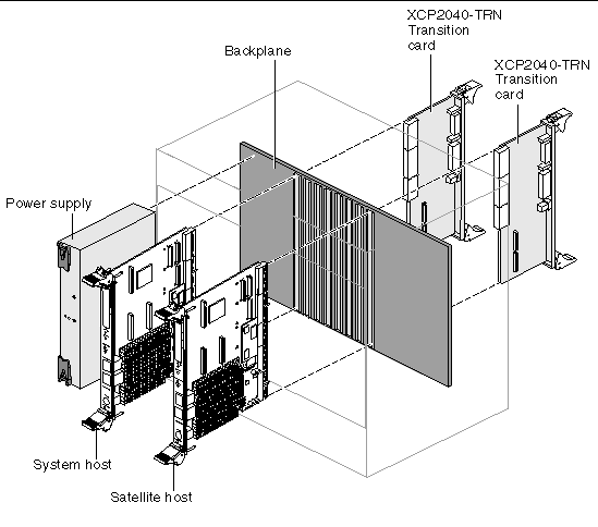
- The transition card must be installed in the slot directly behind the Netra CP2040/CP2140 board. These back-to-back slots have common pins to enable passing of signals between them.
- Ensure that you are installing an XCP2040-TRN I/O Transition Card by checking to see that its part number is 3750120, as described in Determining Part Number, Serial Number, and Revision Number.
- To be in compliance with the NEBS Level 3 Intrabuilding Lightning Surge Tests, (Telecommunications Port) the intrabuilding cabling must be shielded and the shield must be grounded at both ends. Please refer to GR-1089-CORE, Section 4.5.9.
- Refer to Importent Safety Information for Sun Hardware Systems (816-7190-xx) and XCP2040-TRN I/O Transition Card Product Note (816-0898-xx) included in the transition card ship kit for important safety information.

|
Caution - Transition cards built for use with other CompactPCI host boards are not compatible with these Netra boards and might cause damage to themselves, the host, and the backplane if installed.
|
|
 To Install the Transition Card in a CompactPCI Chassis To Install the Transition Card in a CompactPCI Chassis
|
Please read the following instructions before installing the XCP2040-TRN I/O transition card into the CompactPCI system:
1. Ensure that power is disconnected from the chassis.
The transition card and the corresponding Netra board can be installed while the chassis is powered--however only start with a powered chassis if you must do so.
2. Ensure that no host board is installed in front of the rear backplane slot.
When a CompactPCI system is on and running, the transition card must be inserted first, followed by the mating CP2040/CP2140 board. If the CP2040/CP2140 board is already inserted and the system is on, do not insert the transition card into the CompactPCI system.

|
Caution - The XCP2040-TRN I/O transition card is not hot-swappable. Its entire power supply comes from the mating CP2040/CP2140 board (also see Power Requirements).
|
3. Check the positioning of the XCP2040-TRN I/O transition card ejection levers.
Ensure that the XCP2040-TRN I/O transition card ejection levers are aligned perpendicular to the card flange.
4. Connect cables to the following headers before the transition card is inserted into the chassis:
Parallel port header, floppy header, internal SCSI A connector, PS/2 keyboard header and PS/2 mouse header.
|
Note - Cables connecting to the rear panel can be installed after the transition card is in the chassis. These include USB A and B connectors, SCSI A and B connectors, ethernet A and B connectors and serial port A and B connectors.
|
5. Install the XCP2040-TRN I/O transition card into the chassis rear connector slot, as described in the following steps:
a. Position the card such that its J5 connector and the USB B connector on the front panel are on top, as shown in FIGURE 20.
FIGURE 20 Transition Card Alignment During Installation in Backplane
b. Insert the card into the rear slot that aligns directly behind the slot into which you want to install the Netra CP2040/CP2140 board as shown in FIGURE 21.
FIGURE 21 Typical Assembly of the CP2040/CP2140 Board System with Transition Cards
c. Engage the card edges with the chassis card guides and slide the transition card into the chassis, while pushing up on the upper ejection lever, and down on the lower ejection lever. See FIGURE 20.
d. Using the ejection levers, gently maneuver the card toward the backplane, without engaging the card socket with the backplane pins.
At this point, the card rear flange should project approximately 1/4 in. (6 mm) back from the fully home position.

|
Caution - During the next step, ensure that the transition card is perpendicular to the backplane when connecting to the backplane pins. Incorrect vertical or angular positioning during card insertion can result in damage to the backplane and subsequent electrical destruction of the transition card and the corresponding Netra host board.
|
e. Apply pressure to engage the pins and seat the card.
When the card is fully installed, the notches in the ejection levers will be engaged with the ejection lever slots on the chassis.
6. Install the Netra CP2040/CP2140 board into the front of the chassis and push the board towards the backplane to make sure it is seated properly and the connectors make good contact with the transition card.
For further details on installation of the Netra board see the Netra CP2040 Technical Reference and Installation Manual (P/N 806-4994-xx) or the Netra CP2140 Technical Reference and Installation Manual (P/N 816-4908-xx).
7. Install the supported peripheral devices at the transition card connector ports as required.