| XCP2060-TRN I/O Transition Card |
| XCP2060-TRN I/O Transition Card |
|
XCP2060-TRN I/O Transition Card Manual |
The XCP2060-TRN I/O Transition Card (375-0120-xx) is designed to be used with the Netra CP2060/CP2080/CP2160 range of Compact PCI host/satellite boards and is fully compliant with the CompactPCI Core Specification, Release Note for PICMG 2.0 Revision 3.0 (October 1999, PCI Industrial Computers Manufacturers Group).
The XCP2060-TRN I/O Transition Card is a fully compatible, carrier-grade CompactPCI I/O card for the Netra CP2060/CP2080/CP2160 boards. However, it is not compatible with other CompactPCI boards.
It is the responsibility of the system designer to integrate peripheral devices to the connectors on the backplane in a Netra CP2060/CP2080/CP2160 chassis configuration. A designer can either connect directly to the backplane signals or use an XCP2060-TRN I/O Transition Card. This document provides information only for the integration of the XCP2060-TRN I/O Transition Card in a Netra CP2060/CP2080/CP2160 board CompactPCI chassis.
This document contains the following sections:
This section lists the important features of the XCP2060-TRN I/O Transition Card.
The XCP2060-TRN I/O Transition Card requires a CompactPCI chassis with a backplane that accommodates front and rear CompactPCI board installation. The primary purpose of this board is to provide the connection to Netra CP2060/CP2080/CP2160 board I/O devices.
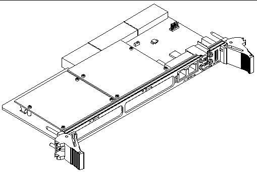
The 6U form factor, single-slot transition card supplies rear I/O connection to support additional peripherals with simplified system cabling for use with the compatible CompactPCI system host boards. The rear I/O access also enables the complementary system host boards to be replaced without disconnecting cables. Industry-standard connectors and pin assignments ensure ease of use and flexible design. The XCP2060-TRN I/O Transition Card enables the creation of high-density systems by enabling easy access to I/O.
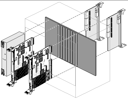
FIGURE 1 shows the XCP2060-TRN I/O Transition Card and a typical Netra CP2160 board connected through the backplane.
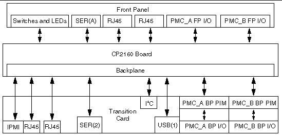
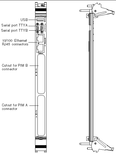
The XCP2060-TRN I/O Transition Card provides additional I/O features (through the J3 and J5 CompactPCI connector interfaces) to the Netra CP2060/CP2080/CP2160 boards. Many I/O functions are provided on the transition card's own faceplate (as shown in FIGURE 2), as well as from headers mounted on the card.
Refer to Cabling Requirements for information on which cables to use for the transition card.
|
When switch closed, write protect is disabled and the I2C EEPROM can be written to.
|
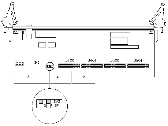
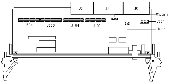
FIGURE 4 shows the location of the on-board components.
The XCP2060-TRN I/O Transition Card is designed to support the Netra CP2060/CP2080/CP2160 host board. It therefore supports the software supported by the host boards. (See the Netra CP2060 and CP2080 Technical Reference Manual and Installation Guide, P/N 806-6658-xx, and the Netra CP2160 CompactPCI Board Installation and Technical Reference Manual, P/N 816-5772-xx, for host board software support.)
This section provides mechanical, electrical, environmental, and other relevant specifications for the XCP2060-TRN I/O Transition Card.
TABLE 2 shows the physical dimensions for the XCP2060-TRN I/O Transition Card.
The XCP2060-TRN I/O Transition Card has mainly passive components. However, some power from the backplane is provided to PIM carriers A and B and to the I2C EEPROM.
For information on PIM allowable dissipation and limits on PIM power consumption, see VITA 36, PMC I/O Module Standard.
For details on the environmental specifications, compliance, and reliability/availability, please see the of the Netra CP2060 and CP2080 Technical Reference Manual and Installation Guide (806-6658-xx) and the Netra CP2160 CompactPCI Board Installation and Technical Reference Manual (816-5772-xx).
For Class B EMI compliance on the XCP2060-TRN I/O Transition Card, note the following cabling requirements:
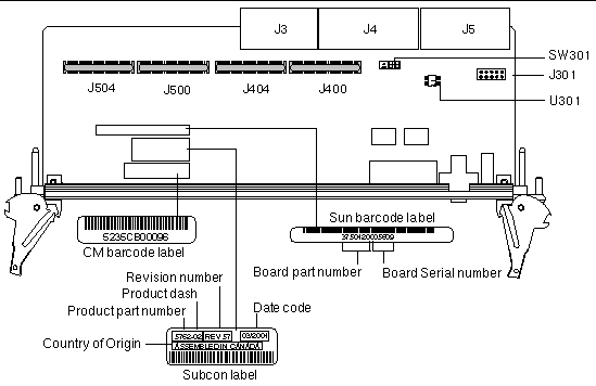
The XCP2060-TRN I/O Transition Card part number, serial number, and revision number can be found on stickers located on the card (see FIGURE 5). For proper identification of the XCP2060-TRN I/O Transition Card, please see the list below along with FIGURE 5.
The Sun Microsystems barcode label provides the following information:
The Subcon label provides the following information:
|
Note - The CM barcode label in FIGURE 5 is an optional label and may or may not appear on the XCP2060-TRN transition card. |
This section lists the pins and signal names of the I/O faceplate connectors on the transition card.
USB connector port A is available on the XCP2060-TRN I/O Transition Card I/O panel. If the user so desires, a second USB connector, port B, is available for use on the faceplate with the addition of a PIM module (that supports a USB connector) on the PIM A connectors.
Two serial ports from the Netra CP2060/CP2080/CP2160 16552 DUART are made available through the rear panel with single-stacked 9-pin connectors. One connector is assigned to Port A and the other connector to Port B. The signal interface of the connector is as follows:
Dual Jack RJ45 Ethernet (J701) AMP1116353-8:
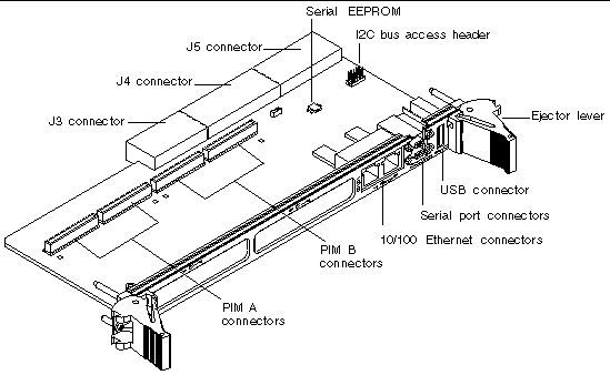
FIGURE 6 shows the on-board interfaces/connectors on the transition card.
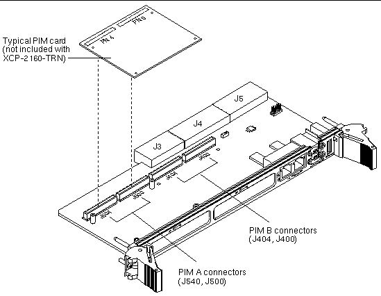
PIM A has two 64 pin connectors at J500 and J504. PIM B has two 64 pin connectors at J400 and J404 (for location see FIGURE 6).
The XCP2060-TRN I/O Transition Card interfaces to the CompactPCI bus through J3 and J5 connectors. The pin assignments for these two sets of connectors are provided in this section.
The pin assignments for J3 Connector are shown in TABLE 12 (for connector location see FIGURE 6).
|
Note - The USR signals are routed from the Netra CP2060/CP2080/CP2160 PMC-A signals. |
The pin assignments for J5 Connector are shown in TABLE 13 (for connector location see FIGURE 6).
The XCP2060-TRN I/O Transition Card is powered through the CP2060/CP2080/CP2160 board (available at 5V/3.3V/12V/-12V, maximum 2.5 W). For more information, see the Netra CP2060 and CP2080 Board Technical Reference Manual and Installation Guide (P/N 806-6658-xx) and the Netra CP2160 CompactPCI Board Installation and Technical Reference Manual (P/N 816-5772-xx).
The XCP2060-TRN I/O Transition Card supports PMC I/O modules (PIMs). PIMs are generally located on transition boards to enable rear I/O from the CompactPCI bus chassis. Custom PIMs can also provide additional I/O that does not fit on the standard transition card faceplate. (For more information on PIM slot mechanics, electrical and logical information, see VITA 36 - PMC I/O Module Standard available at http://www.vita.com and the IEEE P1386 Standard).
The PIM modules are available in two sizes. The single-sized PIMs measure 74 mm (2.92 inches) wide and 69 mm (2.72 inches) deep. The double-sized PIM modules measure 149 mm (5.87 inches) wide and 69 mm (2.72 inches) deep. A double-sized PIM module may also be used in place of two single-sized modules.
FIGURE 7 and FIGURE 8 show typical views of PIM cards used with the XCP2060-TRN I/O Transition Card.
The J5 I/O on the host board, through the PIM cards on the XCP2060-TRN I/O Transition Card, provides matching I/O on the enclosure backpanel. The signals are routed through the CompactPCI J5 connector.
An IHV-supplied PIM card hardware package includes a blank PMC card with no I/O connectors on its faceplate for plugging into the PMC A connectors on the CP2060/CP2080/CP2160 board, and a PIM card that is connected on the XCP2060-TRN I/O Transition Card with I/O connectors available on the (rear) transition card panel. This enables the availability of I/O connections on the rear.
Access to the CP2060/CP2080/CP2160 board SMC serial port via SMC TX and SMC RX signals on both PIMs are available. For details on the PIM connector pins see FIGURE 2.
|
Note - Mount the PIM cards on the XCP2060-TRN I/O Transition Card before the XCP2060-TRN I/O Transition Card is inserted in a CompactPCI system. |
|
Note - The PIM cards shown in FIGURE 7 and FIGURE 8 are examples only and are not included with the XCP2060-TRN I/O Transition Card shipment. |
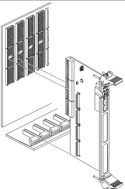
The XCP2060-TRN I/O Transition Card installs into a CompactPCI chassis with a backplane made for front and rear board installation (see FIGURE 9). It must be installed in the slot directly behind the Netra CP2060/CP2080/CP2160 board for proper operation. These back-to-back slots have common pins to enable passing of signals between them.
|
Note - Before installing the transition card, its board part number must be verified to ensure that the correct transition card is being installed into the cPCI system. For information on identification of the transition card, see the section Determining Part Number, Serial Number, and Revision Number, and FIGURE 5 in that section. |
Before installing the XCP2060-TRN I/O Transition Card into a chassis, refer to the safety information in the following documents:
http://www.sun.com/products-n-solutions/hardware/docs/CPU_Boards

|
Caution - Ensure that you are installing an XCP2060-TRN I/O Transition Card. |
You can install the XCP2060-TRN I/O transition card either with the system power on or off. If you are going to install the card with the chassis powered-on, you must install the transition card before the Netra CP2060 or CP2160 board.
1. Disconnect the power from the chassis, if appropriate.
If you must install the transition card with the chassis power on, you must install the transition card before installing the corresponding Netra CP2060 or CP2160 board.
Note that the XCP2060-TRN I/O Transition Card is not hot-swappable.
2. Check the positioning of the XCP2060-TRN I/O Transition Card extraction levers.
Ensure that the XCP2060-TRN I/O Transition Card extraction levers are aligned perpendicular to the card flange.
3. Install the XCP2060-TRN I/O Transition Card into the chassis rear connector slot that lines up directly with the Netra CP2060/CP2080/CP2160 board (see FIGURE 9).
a. Position the card such that its J5 connector is on top.
The USB connector should be uppermost.
b. Engage the board edges with the chassis card guides and slide it into the chassis (see FIGURE 10).
c. Using the ejector handles, gently maneuver the card into registration with the keying hardware and the shoulders surrounding the backplane pins, without the card socket contacts engaging these pins.
At this point, the card rear flange should project approximately 1/4 inch (6 mm) back from the "fully home" position.
d. Apply pressure to engage the pins and seat the board.
4. Install the Netra CP2060/CP2080/CP2160 board into the front of the chassis (see FIGURE 9) and push the board towards the backplane to make sure it is seated properly and the connectors make good contact with the XCP2060-TRN I/O Transition Card.
5. Install the supported peripheral devices at the transition card connector ports as required.
Refer to Cabling Requirements for information on which cables to use for the transition card.
For further details on installation of the Netra board, see the Netra CP2060 and CP2080 Technical Reference Manual and Installation Guide (806-6658-xx) and the Netra CP2160 CompactPCI Board Installation and Technical Reference Manual (816-5772-xx).
Refer to your system manual for instructions on correctly powering-on the system.
|
Note - Step 7 only applies to Netra CP2160 board , not Netra CP2060 or CP2080 boards. |
7. (For CP2160 only) At the ok prompt, set the front-phy? variable to enable the Ethernet ports on the rear transition card as follows:
ok setenv front-phy? false |
This will activate the Ethernet ports on the rear transition card and deactivate the Ethernet ports on the front panel of the Netra CP2160 board.
See the Netra CP2160 Installation and Technical Reference Manual (816-5772-xx) for more information on setting OpenBoot PROM configuration variables.
| XCP2060-TRN I/O Transition Card | 806-6203-11 |
Copyright © 2003, Sun Microsystems, Inc. All rights reserved.


